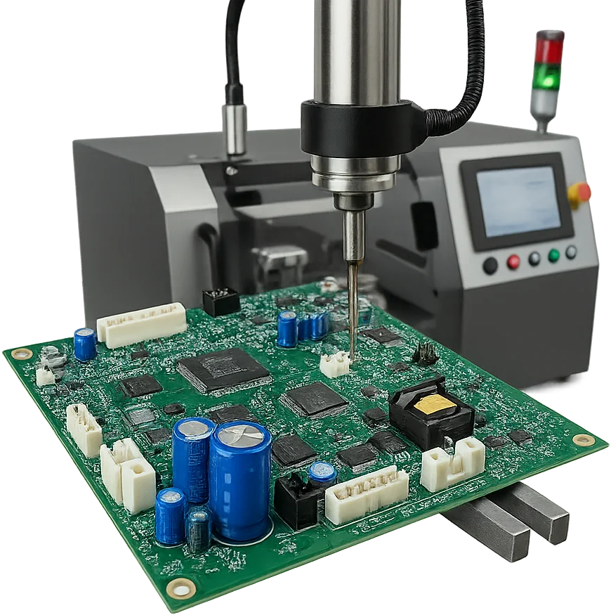
Selecting the right assembly method for high-reliability electronics often requires looking beyond standard Surface Mount Technology (SMT) to the mechanical robustness of Through-Hole Technology (THT). While SMT offers density, through hole soldering basics remain the gold standard for connectors, power components, and assemblies subject to high mechanical stress or vibration. This guide provides a technical playbook for buyers and engineers to define specifications, mitigate process risks, and validate supplier capabilities for THT assembly.
Key Takeaways
- Mechanical Strength: Through-hole joints provide 5–10x the pull strength of surface mount joints, making them essential for I/O connectors and heavy transformers.
- Process Hierarchy: Understand the cost/quality trade-offs between manual soldering (low volume), wave soldering (high volume), and selective soldering (precision mixed technology).
- Thermal Profiling: A critical success factor is the pre-heat phase, typically requiring the PCB to reach 90°C–120°C before hitting the solder wave to activate flux and prevent thermal shock.
- Hole Fill Requirements: IPC Class 2 requires a minimum of 50% vertical barrel fill, while IPC Class 3 demands 75% minimum fill for high-reliability aerospace or medical applications.
- Design for Manufacturing (DFM): Ensure a hole-to-lead clearance of 0.20mm to 0.30mm; too tight prevents solder flow, while too loose causes weak joints and voiding.
- Fixture Necessity: For mixed-technology boards, a wave solder fixture intro is often required to shield SMT parts, adding tooling costs ($200–$500) but ensuring reliability.
- Validation Tip: Do not rely solely on visual inspection; implement X-ray sampling for components with obscured leads (like PGAs) to verify barrel fill percentages.
Scope, Decision Context, and Success Criteria
Defining the scope of through hole soldering basics early in the project prevents costly rework during mass production. Unlike SMT, which is highly automated, THT often involves variable processes depending on component mix and volume.
Success Criteria
To declare a THT project successful, the following metrics must be met:
- Solder Joint Reliability: Zero cold solder joints and compliance with IPC-A-610 (Class 2 or 3) for wetting and fillet shape.
- Throughput Efficiency: First Pass Yield (FPY) exceeding 98.5% at the wave or selective soldering stage to minimize manual touch-up costs.
- Thermal Safety: No thermal damage to adjacent SMT components or the PCB laminate (measling/blistering) due to excessive heat exposure.
Boundary Cases
- Mixed Technology: If a board is 90% SMT and 10% THT, the decision between selective soldering and wave soldering (with pallets) is critical.
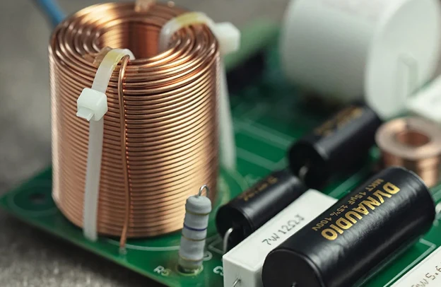
- High Thermal Mass: Components like large heat sinks or heavy copper planes (2 oz+) require specific thermal profiles that differ from standard FR4 assemblies.
Specifications to Define Upfront (Before You Commit)
Clear specifications are the primary defense against quality fade. When requesting a quote or setting up a new product introduction (NPI), explicitly define these parameters.
Critical Specification List
- IPC Classification: Specify IPC-A-610 Class 2 (Standard) or Class 3 (High Reliability). This dictates hole fill and inspection criteria.
- Solder Alloy: SAC305 (Lead-Free) is standard, but SnPb (Leaded) may be required for defense/aerospace.
- Flux Type: No-Clean (leaves residue, usually acceptable) vs. Water-Soluble (requires washing, higher cleanliness).
- Component Lead Length: Post-solder lead length should typically be 1.5mm to 2.5mm max to prevent shorting.
- Annular Ring: Minimum 0.15mm (6 mil) to ensure sufficient mechanical anchor.
- Hole Clearance: +0.25mm (+10 mil) over nominal lead diameter is the ideal target for wave soldering.
- Thermal Relief: Required for holes connected to large copper planes to prevent "cold joints" caused by heat sinking.
- Component Orientation: Orient chips parallel to the wave direction to minimize bridging.
- Keep-out Zones: Define 3mm to 5mm clearance around THT pads if using wave solder pallets.
- Maximum Component Height: Ensure tall capacitors do not interfere with the wave nozzle or machine clearance (typically <15mm for standard setups).
- Board Thickness: Standard is 1.6mm; boards >2.4mm require longer pre-heat and dwell times.
- Pallet Design: If SMT is present on the solder side, specify if a "selective wave pallet" is needed.
Key Parameter Table
| Parameter | Standard Specification | High-Reliability / Class 3 | Why It Matters |
|---|---|---|---|
| Hole Fill (Vertical) | > 50% | > 75% | Determines mechanical pull strength and vibration resistance. |
| Circumferential Wetting | 270° | 330° | Ensures the solder has fully bonded to the lead and barrel. |
| Solder Pot Temperature | 255°C ± 5°C | 255°C ± 2°C | Controls thermal shock and solder fluidity. |
| Contact Time (Dwell) | 2–4 seconds | 3–5 seconds | Sufficient time for solder to wick up the barrel without damaging parts. |
| Pre-heat Temperature | 90°C–110°C (Top side) | 100°C–120°C (Top side) | Activates flux and prevents thermal shock to ceramic components. |
| Flux Application | Spray Fluxer | Drop Jet / Precision Spray | Ensures consistent coverage without excessive residue. |
| Conveyor Speed | 1.0 – 1.2 m/min | 0.8 – 1.0 m/min | Slower speeds allow better capillary action in thick boards. |
| Max Solder Impurities | < 0.3% Copper | < 0.15% Copper | High copper content causes "sluggish" solder and bridging. |
Key Risks (Root Causes, Early Detection, Prevention)
Understanding failure modes in SMT and THT assembly allows buyers to audit suppliers effectively. Here are the top risks associated with through hole soldering basics.
1. Solder Bridging (Shorts)
- Root Cause: Leads too long, pitch too fine (<2.0mm), or insufficient flux application.
- Early Detection: Automated Optical Inspection (AOI) or electrical testing (ICT).
- Prevention: Limit lead protrusion to <2.0mm. Use "solder thief" pads on the trailing edge of connectors.
2. Cold Solder Joints
- Root Cause: Insufficient heat (thermal mass of component > heat input) or oxidation on leads.
- Early Detection: Visual inspection shows dull, grainy, or convex joints.
- Prevention: Increase pre-heat to 110°C. Use thermal relief pads on ground planes.
3. Insufficient Hole Fill
- Root Cause: Flux burnout before wave contact, or hole-to-lead ratio is too tight (<0.15mm).
- Early Detection: X-ray inspection or backlit visual inspection.
- Prevention: Optimize hole size to Lead Diameter + 0.25mm. Check flux activity.
4. Solder Balls
- Root Cause: Moisture in the PCB (outgassing) or excessive flux bursting during wave contact.
- Early Detection: Visual inspection; rattling sound in final assembly.
- Prevention: Bake PCBs at 105°C for 4 hours prior to assembly. Adjust pre-heat ramp rate (<2°C/sec).
5. Blowholes / Pinholes
- Root Cause: Trapped volatiles in the laminate or barrel plating issues.
- Early Detection: Visual inspection reveals small holes in the solder fillet.
- Prevention: Ensure high-quality PCB fabrication with minimum 25µm copper plating in barrels.
6. Lifted Pads
- Root Cause: Excessive heat or mechanical stress during lead trimming or cooling.
- Early Detection: Visual inspection; pad separates from laminate.
- Prevention: Strictly control rework temperatures (<350°C iron tip) and avoid mechanical force on warm pads.
7. Flux Residue Contamination
- Root Cause: Incompatible flux type or insufficient wash cycle.
- Early Detection: Ionic contamination testing (ROSE test).
- Prevention: Validate wash process parameters (water temp >60°C, saponifier concentration).
8. Component Thermal Damage
- Root Cause: Exceeding component thermal rating (e.g., plastic connectors melting).
- Early Detection: Visual deformation or functional failure.
- Prevention: Use a wave solder fixture intro (pallet) to shield sensitive bodies. Verify component specs (must withstand 260°C for 10s).
Validation & Acceptance (Tests and Pass Criteria)
Validation ensures the PCB quality meets the specified IPC class. A robust plan includes both non-destructive and destructive testing.
Acceptance Criteria Table (IPC-A-610)
| Feature | Class 2 Criteria | Class 3 Criteria |
|---|---|---|
| Wetting (Lead & Pad) | Good wetting on pad and lead. | Good wetting; fillet must be concave. |
| Vertical Fill | 50% minimum. | 75% minimum. |
| Solder Protrusion | Visible on secondary side. | Visible on secondary side. |
| Lead Protrusion | Max 2.5mm. | Max 1.5mm (to prevent arcing). |
| Wire/Lead Damage | Minor nicks allowed (<10%). | No nicks or deformation allowed. |
6 Essential Validation Tests
- Visual Inspection (100%): Operators or AOI machines check for bridges, missing solder, and component orientation.
- Automated Optical Inspection (AOI): Cameras verify fillet shape and presence. Essential for high-volume mass production.
- X-Ray Inspection (Sample): Mandatory for checking barrel fill on connectors where the top side is obscured by the connector body.
- Pull/Shear Test (Destructive Sample): Verifies mechanical strength. A typical THT lead should withstand >10N (depending on diameter) before failure.
- Cross-Section Analysis (Micro-sectioning): The ultimate verification for intermetallic compound (IMC) formation and barrel fill. Performed during NPI.
- Ionic Contamination Test (ROSE): Ensures flux residues are removed to prevent corrosion. Limit: <1.56 µg/cm² NaCl equivalent.
Sampling Strategy
- NPI Phase: 100% X-ray and 5-piece cross-section.
- Production: AQL 0.65 for critical defects (shorts), AQL 1.0 for major defects (insufficient fill).
Supplier Qualification Checklist (RFQ, Audit, Traceability)
When evaluating a partner for turnkey assembly, use this checklist to verify their THT capabilities.
Traceability & Process Control
- Does the supplier record solder pot temperature profiles for every batch?
- Is there a log of solder bath analysis (checking for copper/gold embrittlement)?
- Can they trace a specific PCBA serial number to the operator and machine used?
- Is there an automated fluxer (spray) or manual brushing? (Automated is preferred for consistency).
DFM & Engineering
- Do they provide a DFM report specifically for wave soldering (checking pad spacing, orientation)?
- Can they design and fabricate custom wave solder pallets in-house or via a trusted partner?
- Do they have experience with heavy copper PCBs requiring high thermal energy?
Testing Capabilities
- Do they have in-house ICT test capabilities for THT circuits?
- Is X-ray inspection available for barrel fill verification?
- Do they perform daily "profiling" of the wave solder machine using a thermal profiler (e.g., KIC)?
Change Control
- Is there a formal process for changing solder alloys or flux brands?
- Are operators certified to IPC-J-STD-001 standards?
How to Choose (Trade-Offs and Decision Rules)
Deciding between manual, wave, and selective soldering depends on volume, design complexity, and budget.
10 Decision Rules
- If volume is < 50 boards, choose manual soldering (avoids tooling costs).
- If volume is > 500 boards, choose wave soldering (speed and consistency).
- If the board has SMT on both sides + THT, choose selective soldering or wave with pallets.
- If components are taller than 15mm on the solder side, choose selective soldering (wave height limitations).
- If high-precision fill (Class 3) is required on dense connectors, choose selective soldering.
- If budget is tight and design allows, choose wave soldering (lowest cost per joint).
- If using flex PCBs, choose manual or specialized tooling (wave can damage flex).
- If leads are very close (<1.5mm pitch), choose selective soldering to avoid bridging.
- If the PCB is >3mm thick, choose selective soldering with high pre-heat capability.
- If rapid prototyping is needed, choose manual soldering (zero setup time).
FAQ (Cost, Lead Time, DFM Files, Materials, Testing)
Q: How much does a wave solder fixture (pallet) cost? A: Custom pallets typically range from $200 to $600 depending on complexity and material (Durostone/composite). They are reusable for thousands of cycles.
- Protects bottom-side SMT.
- Prevents PCB warping.
- One-time NRE charge.
Q: Can I use through-hole components on a metal core PCB (MCPCB)? A: Yes, but it is difficult due to rapid heat dissipation.
- Requires high-power pre-heating.
- Manual soldering is often preferred for single connectors.
- Design must isolate the hole from the metal core to prevent shorts.
Q: What files are needed for THT assembly? A: Standard Gerber files are sufficient, but specific layers help.
- Drill File: Specifies hole sizes.
- Assembly Drawing: Shows component locations and polarity.
- XY Data: Useful if using automated insertion machines.
Q: Why is "selective soldering" more expensive than wave soldering? A: Selective soldering is slower as it solders point-by-point or row-by-row.
- Machine time is higher per board.
- Programming time is longer.
- However, it eliminates the need for expensive pallets and post-wave manual masking.
Q: How do I prevent "solder balls" on my THT boards? A: Solder balls are often caused by moisture or flux issues.
- Bake PCBs: Remove moisture before assembly.
- Check Flux: Ensure compatible pre-heat temps.
- Solder Mask: Ensure mask dams exist between pads.
Q: What is the difference between "drag soldering" and "dip soldering"? A: These are selective soldering techniques.
- Dip: The nozzle rises and dips the entire group of pins at once (faster).
- Drag: A mini-wave moves across the pins (more precise, slower).
Q: Does THT assembly affect the lead time? A: It can add 1–2 days compared to pure SMT due to the extra process step.
- Manual insertion takes time.
- Wave pallet fabrication (if needed) adds 3–5 days to the initial setup.
Q: Can I use lead-free solder for THT? A: Yes, SAC305 is standard.
- Requires higher temperatures (255°C+).
- Wetting is slightly slower than leaded solder.
- Visual appearance is grainier (this is normal).
Request a Quote / DFM Review for Through Hole Soldering Basics (What to Send)
Glossary (Key Terms)
| Term | Definition |
|---|---|
| Annular Ring | The ring of copper around a plated through-hole. Critical for lead attachment. |
| Wave Soldering | A bulk soldering process where the PCB passes over a wave of molten solder. |
| Selective Soldering | A localized soldering process using a mini-wave nozzle for specific components. |
| Solder Pallet / Fixture | A custom carrier made of heat-resistant material (e.g., Durostone) to mask SMT parts during wave soldering. |
| Flux | A chemical agent that cleans metal surfaces and promotes solder wetting. |
| Pre-heat | The phase of heating the PCB to activate flux and reduce thermal shock before soldering. |
| Wetting | The ability of molten solder to spread and bond to the metal surface. |
| Fillet | The concave shape of the solder joint connecting the lead to the pad. |
| Cold Joint | A defective joint where solder failed to wet properly, often due to low heat. |
| Bridging | An unwanted electrical short created by solder connecting two adjacent pads. |
| Dwell Time | The duration a specific point on the PCB is in contact with the molten solder wave. |
| Thieving Pad | A dummy pad added to the trailing edge of a component footprint to "steal" excess solder and prevent bridging. |
Conclusion (Next Steps)
Mastering through hole soldering basics is about balancing mechanical requirements with manufacturing efficiency. While SMT handles the bulk of modern electronics, THT remains the backbone for power and connectivity. By defining clear specs for hole fill and thermal profiles, and choosing the right partner with validated testing capabilities, you ensure your product withstands the rigors of the real world. Start by reviewing your current BOM for THT components and evaluating if a switch to selective soldering could improve your yield and reliability.