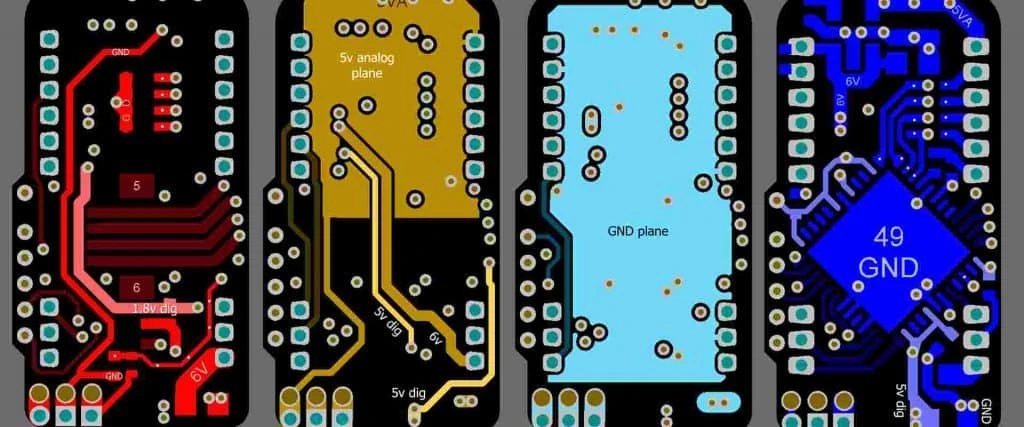
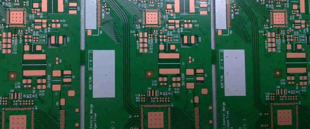
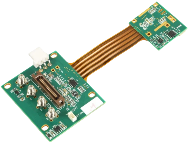
Quantum computing and sensing technologies have moved from theoretical physics labs to engineering reality. However, the fragility of quantum states (qubits) presents a massive manufacturing challenge. Standard electronics packaging is insufficient. It introduces magnetic noise, thermal instability, and chemical contaminants that cause decoherence. This guide details ultra clean packaging for quantum, a specialized manufacturing discipline focused on preserving qubit coherence through material purity, non-magnetic fabrication, and extreme surface cleanliness.
At APTPCB (APTPCB PCB Factory), we understand that a single microgram of magnetic residue or a microscopic void in a solder joint can render a quantum processor useless. This guide covers the entire lifecycle of these critical components, from initial material selection to final validation.
Key Takeaways
Before diving into the technical specifications, here are the critical insights for engineers and procurement teams:
- Magnetic Hygiene is Paramount: Standard PCB finishes like ENIG (Electroless Nickel Immersion Gold) are often forbidden because Nickel is magnetic.
- Surface Roughness Impacts Loss: At microwave frequencies used for qubit control, surface roughness increases dielectric loss.
- Cryogenic Survival: Packaging must survive repeated cooling to millikelvin temperatures without delamination.
- Cleanliness Beyond Visuals: "Ultra clean" refers to chemical purity and the absence of paramagnetic impurities, not just dust.
- Validation is Complex: Standard electrical tests are insufficient; you need residual resistance ratio (RRR) testing and cryogenic verification.
- Material Matching: The Coefficient of Thermal Expansion (CTE) mismatch becomes fatal at near-zero Kelvin.
- APTPCB Approach: We utilize dedicated lines to prevent cross-contamination from standard commercial PCBs.
What ultra clean packaging for quantum really means (scope & boundaries)
Building on the key takeaways, it is essential to define the strict boundaries of this manufacturing category. Ultra clean packaging for quantum is not merely a "high-end" version of a standard printed circuit board. It is a distinct engineering discipline where the packaging enclosure and interconnects become part of the quantum device's Hamiltonian (energy landscape).
In standard electronics, packaging protects the chip. In quantum electronics, the packaging interacts with the chip. If the packaging contains magnetic materials, it distorts the magnetic fields required to manipulate qubits. If the dielectric materials are lossy, they absorb the microwave photons used for computation.
Scope of "Ultra Clean":
- Magnetic Contamination Control: Eliminating ferromagnetic materials (Iron, Nickel, Cobalt) from the substrate, plating, and underfill.
- Chemical Purity: Removing flux residues, organic contaminants, and oxidation that could outgas in a dilution refrigerator (cryostat).
- Surface Integrity: Achieving atomic-level smoothness on conductors to minimize two-level system (TLS) defects.
Boundaries: This guide focuses on the packaging level—the interposer, the PCB substrate, the lid, and the connectors—rather than the fabrication of the qubit chip itself. It bridges the gap between the microscopic quantum chip and the macroscopic control wiring.
ultra clean packaging for quantum metrics that matter (how to evaluate quality)

Once the scope is defined, engineers must quantify "cleanliness" and performance using specific metrics. The following table outlines the critical parameters for ultra clean packaging for quantum.
| Metric | Why it matters | Typical Range / Factor | How to measure |
|---|---|---|---|
| Magnetic Susceptibility | Magnetic impurities cause qubit dephasing and frequency shifts. | < $10^{-5}$ (dimensionless) | SQUID Magnetometry or Vibrating Sample Magnetometer (VSM). |
| Surface Roughness (Ra) | Rough surfaces increase conductor loss at microwave frequencies (skin effect). | < 0.5 µm (for high-Q lines) | Atomic Force Microscopy (AFM) or Profilometer. |
| Dielectric Loss Tangent ($\tan \delta$) | High loss dielectrics absorb quantum signals, reducing coherence time ($T_1$). | < $0.001$ at cryogenic temps | Resonant cavity measurement at 4K or lower. |
| Residual Resistance Ratio (RRR) | Indicates purity of conductive metals (like Copper or Aluminum) at low temps. | > 50 (for high purity Cu) | Ratio of resistance at 300K vs. 4K. |
| Outgassing Rate | Gas release degrades the vacuum in the dilution refrigerator. | < $1.0 \times 10^{-8}$ mbar·L/s | Vacuum chamber mass spectrometry. |
| CTE Mismatch | Differential contraction at 10mK causes cracking or warping. | Match within 2-5 ppm/K | Thermomechanical Analysis (TMA). |
| Plating Thickness Uniformity | Non-uniform plating alters impedance control for microwave pulses. | ± 5% of target thickness | X-Ray Fluorescence (XRF). |
How to choose ultra clean packaging for quantum: selection guidance by scenario (trade-offs)
Understanding the metrics allows us to select the right packaging architecture for specific quantum modalities. There is no "one size fits all" in ultra clean packaging for quantum; every choice involves a trade-off between thermal performance, signal integrity, and manufacturability.
Scenario 1: Superconducting Qubits (Transmon)
- Requirement: Absolute minimum magnetic noise and high thermal conductivity.
- Recommendation: Oxygen-Free High Thermal Conductivity (OFHC) Copper chassis with Silver or direct Gold plating.
- Trade-off: Copper is heavy and oxidizes easily. It requires immediate passivation. Avoid Nickel underplating at all costs.
- APTPCB Tip: Use non-magnetic electroless silver finishes.
Scenario 2: Trapped Ion Processors
- Requirement: Optical access and extremely low RF loss for ion traps.
- Recommendation: Ceramic PCB (Alumina or Aluminum Nitride) with gold-plated tracks.
- Trade-off: Ceramics are brittle and difficult to machine into complex 3D shapes compared to metals.
- Selection Logic: The thermal stability of ceramic outweighs the machining cost.
Scenario 3: Spin Qubits in Silicon
- Requirement: High-density interconnects (HDI) to control many gates in a small area.
- Recommendation: Multi-layer organic substrates (like Rogers or Tachyon) with non-magnetic vias.
- Trade-off: Organic substrates have worse thermal conductivity than ceramics.
- Selection Logic: Density is the priority; thermal management is handled via thermal vias and grounding planes.
Scenario 4: Photonic Quantum Computing
- Requirement: Precision alignment for fiber optics and low thermal shift.
- Recommendation: Kovar or Invar packaging (low CTE) with hermetic sealing.
- Trade-off: Kovar is magnetic. It must be shielded or placed far from sensitive detectors if magnetic fields are involved.
- Selection Logic: Mechanical stability for optical alignment takes precedence.
Scenario 5: Cryogenic CMOS Control Electronics
- Requirement: Heat dissipation and reliable electrical contact at 4K.
- Recommendation: Metal Core PCBs (MCPCB) or heavy copper designs.
- Trade-off: Higher capacitance can limit bandwidth.
- Selection Logic: Removing heat generated by the active electronics is the primary failure mode to avoid.
Scenario 6: Rapid Prototyping / Lab Testing
- Requirement: Fast iteration and lower cost.
- Recommendation: High-frequency laminates (PTFE) with standard non-magnetic connectors (SMP/SMA).
- Trade-off: Higher outgassing and less durability than a fully machined metal enclosure.
- Selection Logic: Speed and flexibility are more important than 10-year reliability for test vehicles.
ultra clean packaging for quantum implementation checkpoints (design to manufacturing)

After selecting the architecture, the focus shifts to the execution of the design. Implementing ultra clean packaging for quantum requires a rigorous checkpoint system to prevent contamination at every stage.
1. Material Sourcing & Verification
- Recommendation: Source raw materials (Copper, Aluminum, Dielectrics) only from certified vendors with purity certificates.
- Risk: "Commercial grade" copper often contains trace iron.
- Acceptance: XRF scan of raw stock before machining.
2. Layout Design for Cryogenics
- Recommendation: Avoid closed loops in ground planes that can trap magnetic flux (flux vortices). Use "star" grounding.
- Risk: Trapped flux creates noise that dephases qubits.
- Acceptance: Design Rule Check (DRC) specifically for superconducting loops.
3. Machining & Fabrication
- Recommendation: Use dedicated coolant and tools. Do not use tools that have previously machined steel or nickel.
- Risk: Cross-contamination of magnetic particles embedding into the soft copper/aluminum surface.
- Acceptance: Surface particle analysis.
4. Surface Plating Strategy
- Recommendation: Use Direct Gold (IG) or Electroless Palladium Immersion Gold (EPIG) if wire bonding is needed. Avoid ENIG.
- Risk: The Nickel layer in ENIG is ferromagnetic and kills coherence.
- Acceptance: Magnetic permeability test on a coupon.
5. Signal Integrity Optimization
- Recommendation: Use High Frequency PCB materials like Rogers 4003C or 3003, but ensure the copper cladding is rolled (smoother) rather than electrodeposited.
- Risk: Rough copper interface increases insertion loss.
- Acceptance: TDR (Time Domain Reflectometry) impedance verification.
6. Cleaning Protocol (The "Ultra Clean" Step)
- Recommendation: Multi-stage cleaning: Ultrasonic solvent bath $\rightarrow$ Acid etch (to remove surface oxides) $\rightarrow$ Plasma cleaning.
- Risk: Residues from machining fluids outgas in the vacuum.
- Acceptance: Contact angle measurement (wettability) or FTIR spectroscopy.
7. Assembly & Soldering
- Recommendation: Use Indium solder or flux-less soldering techniques where possible. If flux is used, it must be aggressively cleaned.
- Risk: Flux residue becomes brittle and cracks at cryogenic temperatures, or remains chemically active.
- Acceptance: Visual inspection under UV light for flux residues.
8. Cryogenic Thermal Cycling Test
- Recommendation: Dip test samples in Liquid Nitrogen (77K) multiple times before final QC.
- Risk: CTE mismatch causes delamination or via fracture.
- Acceptance: Electrical continuity check before and after cycling.
9. Connector Integration
- Recommendation: Use non-magnetic SMPM or SMA connectors with Beryllium Copper contacts (non-magnetic plating).
- Risk: Standard connectors often use nickel underplating on the center pin.
- Acceptance: Magnet test on every connector batch.
10. Final Packaging & Storage
- Recommendation: Vacuum seal in ESD-safe, nitrogen-purged bags immediately after cleaning.
- Risk: Oxidation of copper or silver surfaces in ambient air.
- Acceptance: Humidity indicator card check upon delivery.
ultra clean packaging for quantum common mistakes (and the correct approach)
Even with a checklist, specific errors frequently occur in the transition from standard electronics to quantum packaging. Avoiding these mistakes saves time and expensive materials.
Mistake 1: Assuming "Gold Plated" is Non-Magnetic
- The Error: Specifying "Gold Plating" without restricting the underplate. Most shops default to Nickel/Gold (ENIG) for durability.
- Correct Approach: Explicitly specify "Non-magnetic Electroless Gold" or "Direct Gold over Copper" or "Silver Plating."
Mistake 2: Ignoring the Solder Mask
- The Error: Using standard solder mask over the entire board. Solder masks are organic polymers that can be lossy and outgas.
- Correct Approach: Remove solder mask from RF traces. Use it only where absolutely necessary for bridging prevention, or use specific low-loss cryogenic coatings.
Mistake 3: Overlooking Connector Magnetism
- The Error: Buying high-end PCBs but using standard distribution connectors.
- Correct Approach: Verify the datasheet for "Non-Magnetic" certification. Test with a strong rare-earth magnet before assembly.
Mistake 4: Neglecting Thermal Contraction
- The Error: Designing tight mechanical fits at room temperature.
- Correct Approach: Calculate the shrinkage of PTFE/Copper/Aluminum at 4K. PTFE shrinks significantly more than metal, leading to stress fractures.
Mistake 5: Inadequate Cleaning of Vias
- The Error: Trapped plating chemistry in high-aspect-ratio vias.
- Correct Approach: Use advanced rinsing techniques and bake-out procedures to ensure vias are chemically clean and dry.
Mistake 6: Using Standard FR4
- The Error: Using FR4 for the quantum plane.
- Correct Approach: FR4 is acceptable for DC bias lines far from the qubit, but never for the qubit substrate itself due to high dielectric loss.
ultra clean packaging for quantum FAQ (cost, lead time, materials, testing, acceptance criteria)
To further clarify the procurement and engineering process, here are answers to the most frequent questions regarding ultra clean packaging for quantum.
Q1: How does the cost of ultra clean packaging compare to standard RF packaging? The cost is typically 3x to 10x higher. This premium pays for specialized non-magnetic materials (like high-purity OFHC copper), dedicated machining setups to prevent contamination, and rigorous validation testing like magnetic contamination control checks.
Q2: What is the typical lead time for these custom packages? Lead times usually range from 4 to 8 weeks. Material procurement (especially specialized laminates or pure metals) takes time, and the multi-stage cleaning and plating processes are slower than standard PCB fabrication.
Q3: Can I use standard solder for ultra clean packaging? Generally, no. Standard lead-free solders often contain tin-silver-copper alloys that are acceptable, but the flux is the issue. We recommend Indium solders for cryogenic seals or flux-free soldering processes to prevent outgassing.
Q4: What specific materials are best for the dielectric layer? For microwave frequencies, Rogers RO3003, RO4003C, or Taconic TLY-5 are common due to stable dielectric constants. For the highest performance, Sapphire or High-Resistivity Silicon substrates are used, though they require different processing than standard PCBs.
Q5: How do you perform a cryogenic thermal cycling test during production? We utilize liquid nitrogen (77K) immersion. While not as cold as the final operating temperature (10mK), 77K is sufficient to trigger most CTE mismatch failures (delamination, cracking) that would occur at lower temperatures.
Q6: What are the acceptance criteria for magnetic purity? The industry standard is often a relative magnetic permeability ($\mu_r$) of less than 1.00005. For extremely sensitive applications, we may require batch testing using a magnetometer to ensure no ferromagnetic contaminants were introduced during machining.
Q7: Why is surface roughness so critical for quantum packaging? Current travels on the skin of the conductor at microwave frequencies. If the surface is rough (like standard electrodeposited copper), the current path is longer and more resistive, causing signal loss and heating, which leads to decoherence.
Q8: Does APTPCB handle the final assembly or just the bare board? APTPCB offers both. We can fabricate the bare Ceramic PCB or metal chassis, and we also offer PCBA Testing & Quality services to assemble connectors and interposers in a cleanroom environment.
Q9: How do you handle "outgassing" requirements? We perform a high-temperature vacuum bake-out of the finished boards to drive out volatiles. We avoid materials with high vapor pressures (like certain epoxies or standard solder masks) in the design phase.
Q10: Can you plate gold directly onto copper without nickel? Yes, this is called "Direct Gold" or "Direct Immersion Gold" (DIG). It is challenging because copper diffuses into gold, but for cryogenic applications, diffusion is negligible. Alternatively, we use a non-magnetic barrier layer like Palladium or Silver.
Resources for ultra clean packaging for quantum (related pages and tools)
To support your design process, utilize these related resources from APTPCB:
- Substrate Selection: Explore our High Frequency PCB capabilities for low-loss material options.
- Advanced Materials: Learn about Ceramic PCB technology for superior thermal stability.
- Quality Assurance: Review our Testing & Quality protocols, including X-ray and AOI.
- Design Tools: Use our Impedance Calculator to estimate trace dimensions for 50-ohm lines.
ultra clean packaging for quantum glossary (key terms)
| Term | Definition |
|---|---|
| Decoherence | The loss of quantum information due to interaction with the environment (noise, heat, magnetic fields). |
| Qubit | Quantum Bit; the basic unit of quantum information. |
| Cryostat | A refrigerator capable of reaching cryogenic temperatures (often < 1 Kelvin). |
| Dilution Refrigerator | A specific type of cryostat that uses He-3/He-4 mixing to reach millikelvin temperatures. |
| OFHC Copper | Oxygen-Free High Thermal Conductivity Copper; used for its purity and thermal properties. |
| ENEPIG | Electroless Nickel Electroless Palladium Immersion Gold; a plating finish. Note: Standard Nickel is magnetic. |
| Paramagnetism | A form of magnetism where materials are weakly attracted by an external magnetic field. |
| Outgassing | The release of gas that was dissolved, trapped, frozen, or absorbed in some material. |
| CTE | Coefficient of Thermal Expansion; how much a material changes size with temperature. |
| Skin Effect | The tendency of AC current to flow near the surface of a conductor. |
| TLS (Two-Level Systems) | Microscopic defects in dielectrics that absorb energy and cause qubit loss. |
| Superconductivity | A state where a material has zero electrical resistance (usually at very low temps). |
| Flux Vortex | A quantum of magnetic flux trapped in a superconductor. |
| Interposer | An electrical interface routing between one socket or connection to another. |
Conclusion (next steps)
Achieving ultra clean packaging for quantum is a multidisciplinary challenge that combines materials science, RF engineering, and precision manufacturing. It requires moving beyond standard PCB practices to embrace non-magnetic materials, strict chemical hygiene, and cryogenic validation. Whether you are building superconducting transmon qubits or trapped ion sensors, the packaging is the critical interface between the quantum world and the classical control electronics.
At APTPCB, we specialize in bridging this gap. When you are ready to move from design to prototype, ensure you have the following ready for a DFM (Design for Manufacturing) review:
- Gerber Files: With clear stack-up definitions.
- Material Specs: Explicitly stating "Non-Magnetic" requirements.
- Surface Finish: Defined roughness (Ra) and plating chemistry.
- Test Requirements: Specify if cryogenic thermal cycling test or magnetic contamination control validation is needed.
Ready to fabricate your quantum packaging? Request a Quote today and let our engineering team validate your design for the quantum era.
