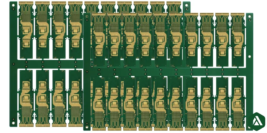
Adopting via in pad (VIP) technology is often a mandatory decision driven by component density, specifically when Ball Grid Array (BGA) pitches drop below 0.5 mm. While this technique maximizes PCB real estate and improves thermal management, it introduces complex plating and filling steps that can jeopardize assembly yields if not strictly controlled. This playbook guides buyers and engineers through the critical specifications, risk mitigation strategies, and acceptance criteria needed to procure reliable VIP boards without manufacturing delays.
Highlights
- Core Benefit: Enables routing for fine-pitch BGAs (< 0.5 mm) and reduces inductance.
- Critical Spec: Cap plating thickness must be controlled (typically 12–15 µm) to ensure a flat surface.
- Primary Risk: "Dimpling" or voids in the via fill, leading to solder joint failure during assembly.
- Validation: Requires IPC Class 3 compliant microsections to verify wrap plating and fill integrity.
Key Takeaways
- Core Benefit: Enables routing for fine-pitch BGAs (< 0.5 mm) and reduces inductance.
- Critical Spec: Cap plating thickness must be controlled (typically 12–15 µm) to ensure a flat surface.
- Primary Risk: "Dimpling" or voids in the via fill, leading to solder joint failure during assembly.
- Validation: Requires IPC Class 3 compliant microsections to verify wrap plating and fill integrity.
- Scope, Decision Context, and Success Criteria
- Manufacturing Capabilities & Ordering Logistics
- Specifications to Define Upfront (Before You Commit)
Contents
- Scope, Decision Context, and Success Criteria
- Manufacturing Capabilities & Ordering Logistics
- Specifications to Define Upfront (Before You Commit)
- Key Risks (Root Causes, Early Detection, Prevention)
- Validation & Acceptance (Tests and Pass Criteria)
- Supplier qualification checklist (RFQ, audit, traceability)
- How to Choose (Trade-Offs and Decision Rules)
- FAQ (cost, lead time, DFM files, materials, testing)
Scope, Decision Context, and Success Criteria
Via in pad manufacturing places a plated through-hole (PTH) directly into a component landing pad, which is then filled with epoxy and plated over ("capped") to create a flat solderable surface. This process, often referred to as VIPPO (Via-in-Pad Plated Over), is distinct from standard tented vias.
When to Use Vip
You typically cross the threshold into VIP territory when:
- BGA Pitch: The component pitch is 0.5 mm or less, leaving insufficient space for dog-bone fanout routing.
- Thermal Requirements: High-power components require direct thermal paths to inner planes (thermal vias).
- High-Speed Signals: Reducing stub length and inductance is critical for signal integrity.
Success Criteria
To consider a VIP project successful, the manufactured boards must meet three measurable outcomes:
- Surface Planarity: The "dimple" (depression) over the filled via must not exceed 15 µm (for Class 3) or 25 µm (for Class 2) to prevent BGA voiding.
- Plating Integrity: The cap plating must not separate from the underlying via plating or fill material during reflow (260°C).
- Fill Completeness: Voids within the epoxy fill must be less than 5% of the via volume to prevent outgassing and "popcorning."
Boundary Cases (When Not to Use Vip)
- Cost Sensitivity: VIP adds 15–25% to the bare board cost due to extra drilling, plating, and planarization steps. If standard dog-bone routing fits, avoid VIP.
- Large Pitch Components: For pitches > 0.65 mm, standard open vias are usually sufficient and lower risk.
Manufacturing Capabilities & Ordering Logistics
Before finalizing your design, verify that the manufacturer's capabilities align with your density requirements. Via in pad manufacturing requires specialized vacuum plugging machines and planarization equipment.
Capability Snapshot
The following table outlines standard versus advanced capabilities for VIP production.
| Parameter | Standard Capability | Advanced Capability | Notes |
|---|---|---|---|
| Min Mechanical Drill | 0.20 mm (8 mil) | 0.15 mm (6 mil) | Smaller drills increase plating difficulty. |
| Max Aspect Ratio | 8:1 | 10:1 | Ratio of board thickness to drill diameter. |
| Pad Diameter (Outer) | Drill + 0.25 mm | Drill + 0.20 mm | Critical for annular ring retention. |
| Plug Material | Non-conductive Epoxy | Conductive / Copper Paste | Non-conductive is preferred for CTE matching. |
| Cap Plating Thickness | 12 µm | > 25 µm | Thicker caps improve flatness but add time. |
| Dimple Depth | < 25 µm | < 15 µm | Critical for fine-pitch BGA assembly. |
| Wrap Plating | Class 2 (> 12 µm) | Class 3 (> 25 µm) | Essential for joint reliability. |
| Layer Count | 4–12 Layers | 14–30+ Layers | Higher layers require stricter registration. |
| Surface Finish | ENIG, OSP | ENEPIG, Hard Gold | ENIG is standard for flat pads. |
| Blind/Buried Vias | Supported | Stacked Microvias | VIP often combines with HDI structures. |
Lead Time & Moq
VIP adds processing steps (filling, baking, planarizing, capping) that extend standard lead times.
| Order Type | Typical Lead Time | MOQ | Key Drivers |
|---|---|---|---|
| Prototype (NPI) | 5–8 Days | 5 Panels | Extra plating cycles and cure times prevent "quick turn" (24h). |
| Small Batch | 10–12 Days | 10–50 Panels | Vacuum plugging setup and cross-section verification. |
| Mass Production | 15–20 Days | > 50 m² | Batch size optimization and capacity planning. |
Specifications to Define Upfront (Before You Commit)
Ambiguous data packages are the leading cause of VIP failure. You must explicitly define the via structure in your fabrication notes and Gerber files. Do not rely on the manufacturer to "guess" which vias need filling.
Critical Parameters Table
Define these values in your fabrication drawing:
| Parameter | Recommended Range | Why it Matters |
|---|---|---|
| Via Type | IPC-4761 Type VII | Specifies filled and capped vias (VIPPO). |
| Drill Diameter | 0.15 mm – 0.25 mm | Large vias (>0.3mm) are difficult to fill without sagging/dimpling. |
| Fill Material | Non-conductive Epoxy (e.g., Taiyo THP-100) | Matches CTE of FR4 better than conductive pastes; reduces stress. |
| Wrap Plating | Min 25 µm (Class 3) | Ensures the knee of the via doesn't crack during expansion. |
| Cap Plating | 12 µm – 15 µm | Provides sufficient copper for soldering without over-plating features. |
| Annular Ring | Min 0.076 mm (3 mil) | Allows for drill wander; vital for IPC Class 2 compliance. |
| Clearance | 0.15 mm | Distance from via pad to nearest copper feature. |
| Solder Mask | LPI (Liquid Photoimageable) | Must not encroach on the capped pad (1:1 opening or defined clearance). |
Detailed Requirements Checklist
- File Identification: Create a separate drill file or layer specifically for VIP holes. Label it clearly (e.g.,
Drill_VIP_Filled.drl). - Aspect Ratio Limit: Keep the aspect ratio (Board Thickness : Drill Diameter) below 10:1. Ratios above 10:1 make it difficult to plate the barrel center and fill completely without voids.
- Etch Compensation Planning: Explicitly state the finished copper weight. The manufacturer must apply etch compensation planning (typically increasing features by 12–25 µm) to account for the multiple etching cycles required in the VIP process.
- Material Tg: Use High-Tg materials (Tg > 170°C) for VIP boards. The extra thermal excursions during manufacturing (baking the fill) stress the laminate.
- Planarity Spec: Specify "Pad flatness to be within 0.001 inch (25 µm) across the BGA array."
Key Risks (Root Causes, Early Detection, Prevention)
Via in pad manufacturing introduces failure modes that do not exist in standard PCBs. Understanding these risks allows you to audit the supplier's process effectively.
1. Dimpling (the "Divot" Effect)
- Root Cause: The epoxy fill shrinks during curing, or the planarization process removes too much copper cap.
- Numeric Limit: Depth > 25 µm is a fail for most fine-pitch BGAs.
- Early Detection: 3D profilometry or cross-sectioning on test coupons.
- Prevention: Use a two-step filling process and ensure the "scrubbing" (planarization) is calibrated. Specify a minimum cap plating thickness.
2. Voids in via Fill
- Root Cause: Air trapped in the via barrel during the plugging process, often due to high aspect ratios or improper vacuum pressure.
- Numeric Limit: Voids > 5% of via volume or any void bridging the barrel wall.
- Early Detection: X-ray inspection (2D or 3D) of the production panel.
- Prevention: Require vacuum plugging technology (not screen printing) for aspect ratios > 6:1.
3. Wrap Plating Separation
- Root Cause: Poor adhesion between the initial electroless copper and the subsequent wrap plating, or thermal shock.
- Numeric Limit: 0% separation allowed at 1000x magnification.
- Early Detection: Thermal stress test (solder float) followed by microsection.
- Prevention: Ensure the supplier performs a "desmear" and proper surface activation before plating.
4. Barrel Cracks (Corner Cracks)
- Root Cause: CTE mismatch between the epoxy fill (CTE ~30-60 ppm) and the copper barrel (CTE ~17 ppm) during reflow.
- Numeric Limit: No cracks extending > 10% through the plating wall.
- Early Detection: Interconnect Stress Testing (IST) or thermal cycling coupons.
- Prevention: Use non-conductive fill (matched CTE) rather than conductive fill, which ironically has worse thermal expansion properties for this application.
Validation & Acceptance (Tests and Pass Criteria)
You cannot verify via in pad quality with a simple visual inspection. You must mandate specific destructive and non-destructive tests.
Acceptance Criteria Table
| Test Item | Method | Pass Criteria | Sampling Rate |
|---|---|---|---|
| Microsection (Cross-section) | IPC-TM-650 2.1.1 | Wrap plating > 25 µm (Class 3); No separation; Cap > 12 µm. | 1 per lot / panel |
| Solderability | J-STD-003 | 95% coverage; no dewetting on capped pads. | 2 coupons per lot |
| Planarity Check | Laser Profilometry / Microscope | Dimple depth < 25 µm (or 15 µm if specified). | 5 spots per panel |
| Void Inspection | X-Ray | No voids > 5% volume; no voids at hole center. | AQL 1.0 |
| Thermal Stress | IPC-TM-650 2.6.8 | No lifting, blistering, or barrel cracks after 6x reflow sim. | 1 coupon per lot |
| Surface Inspection | AOI Data Analytics | Automated check for cap presence and pad diameter consistency. | 100% of panels |
The Role of AOI Data Analytics
Modern manufacturers use AOI data analytics not just to find shorts/opens, but to measure the consistency of the capped pad diameters. If the planarization process is too aggressive, it can reduce the annular ring of the capped via. Analyzing this data helps predict if the batch is drifting out of tolerance.
Supplier Qualification Checklist (RFQ, Audit, Traceability)
When vetting a supplier for via in pad manufacturing, use this checklist to ensure they have the specific equipment and processes required.
Equipment & Process
- Vacuum Plugging Machine: Do they have dedicated vacuum ink plugging equipment (e.g., ITC, Mass)? Screen printing is acceptable only for low aspect ratios.
- Planarization Line: Do they have a ceramic brush or chemical-mechanical planarization (CMP) line for removing excess fill and copper?
- Plating Tanks: Are the plating lines capable of "pulse plating" (helps with high aspect ratio throwing power)?
- X-Ray Capacity: Do they have in-house X-ray for void detection?
Quality & Traceability
- IPC Class Compliance: Can they certify to IPC-6012 Class 3 for VIPPO features?
- Cross-Section Reports: Will they provide a microsection report specifically showing the via fill and cap interface for every shipment?
- Material Control: Do they stock the specific plugging ink defined (e.g., Taiyo THP-100) or an approved equivalent?
- Change Control: Do they agree to notify you before changing the fill material or plating chemistry?
DFM Support
- Pre-CAM Review: Do they offer a DFM report that specifically checks for "etch traps" and annular ring violations on VIP layers?
- Drill File Handling: Do they have a process to merge/separate VIP drills from standard drills if the data is combined?
How to Choose (Trade-Offs and Decision Rules)
Use these decision rules to navigate the trade-offs between cost, reliability, and density.
- If BGA pitch is < 0.5 mm: Choose VIPPO. Standard dog-bone routing is mathematically impossible or too risky for shorts.
- If BGA pitch is ≥ 0.8 mm: Choose Standard Tented Vias. VIP is unnecessary cost (20% premium).
- If thermal management is the only goal: Choose VIP with Conductive Fill (rare) or simply use dense arrays of standard thermal vias if space permits. Note: Non-conductive fill with copper plating is usually better for reliability than conductive fill.
- If the board is High-Frequency (RF): Choose VIP to minimize signal stubs, but verify the dielectric constant of the fill material.
- If cost is the primary driver: Redesign the BGA fanout to avoid VIP if possible (e.g., reduce layer count or increase board size).
- If reliability (Class 3) is paramount: Specify Non-Conductive Fill + Cap. Avoid conductive fill due to CTE mismatch risks.
- If aspect ratio is > 10:1: Redesign the stackup. VIP manufacturing yield drops significantly above this ratio.
- If lead time is tight (< 5 days): Avoid VIP. The curing and planarization steps are physical bottlenecks that cannot be rushed without risking outgassing.
- If the component is a QFN with a center pad: Use VIP on the center pad to prevent solder wicking down open vias, which causes poor thermal bonding.
- If you see "dimples" in prototypes: Tighten the spec to < 15 µm and request a review of the planarization process for production.
FAQ (Cost, Lead Time, DFM Files, Materials, Testing)
Q: How much does via in pad manufacturing increase the PCB cost? A: Typically 15% to 25% over a standard PCB. This covers the extra steps: drilling separate VIP holes, vacuum filling, baking (curing), planarizing (scrubbing), and the secondary plating cycle (capping).
Q: Should I use conductive or non-conductive fill? A: Use non-conductive fill (epoxy) for 95% of applications. It matches the CTE of the laminate better, reducing barrel cracks. Conductive fill offers negligible thermal advantage because the copper plating on the barrel wall conducts most of the heat.
Q: What is the minimum pitch for VIP? A: VIP can support BGA pitches down to 0.35 mm or 0.4 mm. At these pitches, the drill size usually drops to 0.15 mm (6 mil) or 0.125 mm (5 mil), requiring advanced laser drilling or mechanical micro-drilling.
Q: Why do I need separate drill files for VIP? A: It prevents manufacturing errors. If VIP holes are mixed with standard holes, the manufacturer might accidentally fill holes that should be open (like component holes) or miss filling the VIPs, leading to assembly solder theft.
Q: Can I use VIP on just one side of the board? A: Yes, but the process generally applies to the whole panel. The filling and plating steps are global, so while you can design VIPs on one side, the manufacturing flow usually processes the entire board structure.
Q: What happens if the "dimple" is too deep? A: Solder paste can become trapped in the dimple, or the BGA ball may not make contact with the pad shoulders. This leads to voids in the solder joint or open circuits (head-in-pillow defects).
Q: How does VIP affect signal integrity? A: It generally improves it. By placing the via directly in the pad, you eliminate the trace length (stub) between the pad and the via, reducing inductance and capacitance, which is critical for high-speed signals.
Q: What is the difference between Tented Vias and VIP? A: Tented vias are covered with solder mask only (no fill, no cap). VIPs are filled with solid epoxy and plated over with copper. Tented vias cannot be soldered onto; VIPs can.
Request a Quote / DFM Review for via in Pad Manufacturing (What to Send)
To get an accurate quote and a meaningful DFM review, ensure your RFQ package includes:
- Gerber Files (RS-274X) or ODB++: ODB++ is preferred as it distinguishes via types intelligently.
- Separate Drill File: Clearly labeled for filled vias (e.g.,
VIP_Drill.drl). - Fab Drawing / Readme:
- Explicitly state: "IPC-4761 Type VII (Filled and Capped)."
- Specify fill type: "Non-conductive epoxy."
- Specify acceptance criteria: "Dimple depth < 0.025 mm."
- Stackup Diagram: Indicate which layers the VIPs connect (especially for blind/buried structures).
- Quantity: Prototype (e.g., 10 pcs) vs. Production (e.g., 1000 pcs).
- Lead Time Requirement: Acknowledge that VIP requires +2–4 days over standard.
- IPC Class: Class 2 (Standard) or Class 3 (High Reliability).
- Assembly Data (Optional but recommended): Centroid file and BOM if you want the manufacturer to check BGA footprint compatibility.
Glossary (Key Terms)
| Term | Definition |
|---|---|
| VIPPO | Via-in-Pad Plated Over. The industry standard term for a via that is filled and capped with copper. |
| Aspect Ratio | The ratio of the PCB thickness to the diameter of the drilled hole. Critical for plating capability. |
| Dimple | The depression or concave surface at the top of a filled via. Must be minimized for assembly. |
| Planarization | The mechanical or chemical process of leveling the board surface after filling and before capping. |
| Wrap Plating | Copper plating that |
Conclusion
via in pad manufacturing is easiest to get right when you define the specifications and verification plan early, then confirm them through DFM and test coverage.
Use the rules, checkpoints, and troubleshooting patterns above to reduce iteration loops and protect yield as volumes increase.
If you’re unsure about a constraint, validate it with a small pilot build before locking the production release.