Definition, scope, and who this guide is for
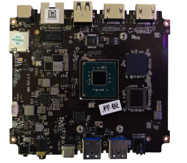
A Video Scaler PCB is the hardware foundation designed to support integrated circuits (ASICs or FPGAs) that convert video signals from one resolution or format to another. Unlike standard logic boards, these PCBs must handle high-bandwidth data streams—such as HDMI 2.1, 12G-SDI, or DisplayPort—while maintaining strict signal integrity during the scaling process. The board layout dictates whether the final video output is artifact-free or suffers from jitter, skew, and electromagnetic interference (EMI).
This playbook is written for hardware engineers, procurement leads, and product managers responsible for sourcing high-performance video hardware. It moves beyond basic fabrication notes to cover the specific architectural decisions required for video processing. You will find actionable specifications, risk mitigation strategies, and validation protocols to ensure your board performs reliably in professional AV, medical imaging, or broadcast environments.
We focus on the critical decision points between design and manufacturing. Whether you are prototyping a new Video Analytics PCB or scaling production for a commercial Video Converter PCB, the physics of high-speed video signals remain the primary constraint. APTPCB (APTPCB PCB Factory) provides this guide to help you align your design intent with manufacturing capabilities before you commit to a production run.
When to use Video Scaler PCB (and when a standard approach is better)
Understanding the definition of a video scaler board leads directly to knowing when specialized manufacturing techniques are required versus when standard processes suffice.
Use a specialized Video Scaler PCB approach when:
- High Bandwidth is Critical: Your design involves 4K, 8K, or high-frame-rate video where signal frequencies exceed 1GHz.
- FPGA Integration: You are using high-pin-count FPGAs (BGA packages) to handle scaling algorithms, requiring High Density Interconnect (HDI) technology.
- Mixed Signals: The board combines sensitive analog video inputs with high-speed digital scaling logic, requiring strict isolation.
- Low Latency: Applications like live broadcasting or medical surgery require minimal signal loss, demanding low-loss dielectric materials.
Stick to a standard PCB approach when:
- Low Resolution: The device handles only standard definition (SD) or basic 720p/1080p signals with low refresh rates.
- Integrated Modules: You are using a pre-certified System-on-Module (SoM) for video processing and only need a carrier board for low-speed connectivity.
- Cost Sensitivity: The project is a consumer-grade toy or basic display where occasional signal artifacts are acceptable to lower the BOM cost.
Video Scaler PCB specifications (materials, stackup, tolerances)
Once you determine that a specialized approach is necessary, you must define the physical parameters that control signal integrity.
- Base Material (Laminate):
- High-Speed Digital: Panasonic Megtron 6 or Isola I-Speed for 12G-SDI/HDMI 2.1 applications.
- Standard HD: High-Tg FR4 (Tg > 170°C) like Isola 370HR for 1080p/4K 30Hz.
- Dk/Df: Dielectric Constant (Dk) < 3.8; Dissipation Factor (Df) < 0.005 @ 10GHz.
- Layer Stackup:
- Count: Typically 8 to 14 layers to accommodate impedance-controlled routing and power planes.
- Symmetry: Balanced copper distribution to prevent warpage during reflow.
- Reference Planes: Solid ground planes adjacent to every high-speed signal layer.
- Impedance Control:
- Single-ended: 50Ω ± 5% (for SDI/clock lines).
- Differential: 90Ω ± 5% (USB/PCIe) or 100Ω ± 5% (HDMI/DP).
- Trace Width/Space: Minimum 3.5mil/3.5mil for HDI designs.
- Via Technology:
- Types: Through-hole, Blind, and Buried vias.
- Backdrilling: Required for signals > 5Gbps to remove via stubs that cause signal reflection.
- Aspect Ratio: 10:1 standard; up to 16:1 for advanced fabrication.
- Surface Finish:
- Preferred: ENIG (Electroless Nickel Immersion Gold) or ENEPIG for flat pads on fine-pitch BGAs.
- Avoid: HASL (too uneven for dense scalers).
- Copper Weight:
- Signal Layers: 0.5 oz or 1 oz (H oz plated up).
- Power Layers: 1 oz or 2 oz to handle current for power-hungry FPGA scalers.
- Soldermask:
- Color: Matte Green or Black (Matte reduces glare for automated optical inspection).
- Clearance: 1:1 or slightly larger than pads (solder dam minimum 3-4 mil).
- Thermal Management:
- Thermal Vias: Under the main scaler IC/FPGA.
- Heat Sink: Dedicated mounting holes or copper keep-out zones for heatsink attachment.
Video Scaler PCB manufacturing risks (root causes and prevention)
Defining specifications is only half the battle; you must also anticipate where the manufacturing process might fail these specifications.
Impedance Mismatch (Signal Reflection)
- Root Cause: Variation in dielectric thickness or trace width etching during production.
- Detection: TDR (Time Domain Reflectometry) coupons fail.
- Prevention: Specify "Impedance Controlled" on the fab drawing and allow the manufacturer to adjust trace width slightly (<10%) to hit the target ohm value.
Signal Skew (Timing Errors)
- Root Cause: Glass weave effect (fiberglass bundles in the PCB material align with traces, changing signal speed).
- Detection: Eye diagram collapse in post-assembly testing.
- Prevention: Use "spread glass" weaves (1067/1078) or route differential pairs at a slight angle (zigzag) relative to the weave.
BGA Voiding (Open Circuits)
- Root Cause: Improper reflow profile or trapped volatiles in the laminate for large scaler chips.
- Detection: X-Ray inspection.
- Prevention: Use high-quality baking procedures for moisture removal before assembly; optimize stencil aperture design.
Via Stub Resonance (Signal Attenuation)
- Root Cause: Unused portion of a plated through-hole acts as an antenna.
- Detection: High insertion loss at specific frequencies (notch filter effect).
- Prevention: Implement controlled depth backdrilling on high-speed lines.
Thermal Warpage (Component Stress)
- Root Cause: Unbalanced copper stackup or low Tg material.
- Detection: Bow and twist measurement; BGA corner cracking.
- Prevention: Ensure symmetrical stackup; use High-Tg materials (>170°C).
CAF (Conductive Anodic Filament) Growth
- Root Cause: Electrochemical migration between vias in high-voltage or high-humidity environments.
- Detection: Long-term reliability testing (shorts develop over time).
- Prevention: Use CAF-resistant materials and maintain minimum wall-to-wall spacing specifications.
Crosstalk (Video Artifacts)
- Root Cause: High-speed video traces routed too close to aggressive clock signals.
- Detection: Visual artifacts or "sparkles" in the video output.
- Prevention: Enforce the "3W rule" (spacing = 3x trace width) for critical signals; use ground stitching vias.
Plating Overhang (Etch Traps)
- Root Cause: Aggressive etching on fine lines leaving slivers.
- Detection: AOI (Automated Optical Inspection).
- Prevention: strict process control on etching rate; design for manufacturability (DFM) review of trace spacing.
Video Scaler PCB validation and acceptance (tests and pass criteria)

To ensure the risks identified above have been mitigated, a rigorous validation plan must be executed before accepting the shipment.
- Impedance Verification (TDR):
- Objective: Confirm trace impedance matches design (e.g., 100Ω).
- Method: Time Domain Reflectometry on test coupons.
- Criteria: Pass if within ±5% or ±10% as specified.
- Signal Integrity (VNA):
- Objective: Measure insertion loss and return loss.
- Method: Vector Network Analyzer on critical paths (if accessible) or dedicated test structures.
- Criteria: Loss < -1.5dB per inch @ Nyquist frequency (context dependent).
- Microsection Analysis:
- Objective: Verify layer stackup, copper thickness, and via quality.
- Method: Cross-sectioning a sample board.
- Criteria: No plating cracks; dielectric thickness matches stackup report; registration within tolerance.
- Solderability Test:
- Objective: Ensure pads will accept solder during assembly.
- Method: Dip and look / Wetting balance test.
- Criteria: >95% coverage; continuous smooth coating.
- Thermal Stress Test:
- Objective: Simulate reflow conditions.
- Method: Solder float test (288°C for 10 seconds).
- Criteria: No delamination, blistering, or measles.
- Ionic Contamination:
- Objective: Prevent corrosion and leakage.
- Method: ROSE testing (Resistivity of Solvent Extract).
- Criteria: < 1.56 µg/cm² NaCl equivalent.
- Electrical Continuity/Isolation:
- Objective: Detect shorts and opens.
- Method: Flying probe or Bed of Nails (ICT).
- Criteria: 100% Pass; no open/short circuits.
- Warpage Measurement:
- Objective: Ensure flatness for BGA assembly.
- Method: Shadow Moiré or feeler gauge on surface plate.
- Criteria: Bow/Twist < 0.75% (IPC Class 2) or < 0.5% (for fine pitch BGA).
Video Scaler PCB supplier qualification checklist (RFQ, audit, traceability)
Validation starts with selecting the right partner. Use this checklist to vet suppliers for high-performance video boards.
RFQ Inputs (What you must send):
- Gerber Files (RS-274X): Complete set including drill files.
- IPC Netlist: For electrical test verification.
- Stackup Drawing: Explicitly stating material type (e.g., "Megtron 6 or equivalent") and layer order.
- Impedance Table: Listing layer, trace width, and target impedance.
- Drill Drawing: Identifying backdrill locations and via types (blind/buried).
- Fab Notes: Specifying IPC Class (2 or 3), color, finish, and tolerances.
- Panelization: If required for your assembly line.
- Volume: Prototype quantity vs. EAU (Estimated Annual Usage).
Capability Proof (What they must show):
- HDI Experience: Proven track record with blind/buried vias and microvias.
- Material Stock: Do they stock high-speed laminates (Rogers, Isola, Panasonic) or order on demand?
- Backdrilling: In-house capability with depth control tolerance < ±0.1mm.
- Fine Line/Space: Capability for 3mil/3mil or tighter.
- Aspect Ratio: Ability to plate high aspect ratio vias (e.g., 12:1 or higher).
- Engineering Support: Do they offer pre-production CAM/DFM review?
Quality System & Traceability:
- Certifications: ISO 9001 is mandatory; UL listing for flammability.
- IPC Standards: Adherence to IPC-6012 (Rigid PCB Performance).
- Cross-Section Reports: Are these provided with every shipment?
- TDR Reports: Are impedance reports generated for every batch?
- Material Certs: Can they provide CoC (Certificate of Conformance) for the laminate?
- AOI: Is Automated Optical Inspection used on inner layers?
Change Control & Delivery:
- PCN Policy: Will they notify you before changing materials or manufacturing location?
- Lead Time: Is the lead time for standard vs. quick-turn clearly defined?
- Packaging: Vacuum sealed with desiccant and humidity indicator cards (HIC).
- Data Security: How do they protect your IP?
How to choose Video Scaler PCB (trade-offs and decision rules)
Even with a qualified supplier, you will face design trade-offs. Here is how to navigate them based on your specific video application.
- Material Cost vs. Signal Integrity
- Rule: If your frequency is > 5GHz (e.g., 4K/8K video), choose Low-Loss Material (Megtron 6).
- Rule: If your frequency is < 3GHz (e.g., 1080p), High-Tg FR4 is sufficient and cheaper.
- HDI vs. Through-Hole
- Rule: If using a 0.5mm pitch BGA scaler, you must use HDI (microvias).
- Rule: If using a 0.8mm or larger pitch, Through-Hole is cheaper and easier to manufacture.
- Backdrilling vs. Blind Vias
- Rule: If you need to remove stubs on a thick board but want to avoid the cost of sequential lamination, choose Backdrilling.
- Rule: If density is the primary constraint, choose Blind/Buried Vias.
- Surface Finish: ENIG vs. OSP
- Rule: If reliability and shelf life are priorities, choose ENIG.
- Rule: If cost is the only driver and assembly is immediate, OSP is acceptable (but risky for complex scalers).
- Application Specifics
- Rule: For a
Video Detection PCB(surveillance), prioritize reliability and environmental protection (conformal coating). - Rule: For a
Video Editor PCB(studio console), prioritize signal latency and noise immunity. - Rule: For a
Video Generator PCB(test equipment), prioritize absolute impedance accuracy (Class 3 tolerance).
- Rule: For a
Video Scaler PCB FAQ (cost, lead time, design for manufacturability (DFM) files, materials, testing)
Q: What is the primary cost driver for a Video Scaler PCB? A: The layer count and material choice are the biggest factors. Moving from FR4 to high-speed materials like Rogers or Megtron can double the laminate cost, and adding HDI layers increases lamination cycles.
Q: How does lead time for Video Scaler PCB differ from standard boards? A: Standard boards take 3-5 days; Video Scaler PCBs often take 8-12 days. This is due to extra steps like backdrilling, impedance testing, and potentially waiting for specialized laminate stock.
Q: What DFM files for Video Scaler PCB are most critical? A: The stackup definition and drill files are critical. You must provide a clear stackup showing dielectric heights to ensure the manufacturer can calculate impedance correctly before etching.
Q: Can I use standard FR4 materials for Video Scaler PCB? A: Only for lower resolutions (up to 1080p/3Gbps). For 4K (12Gbps) and above, standard FR4 has too much signal loss (attenuation), requiring low-loss materials.
Q: What testing for Video Scaler PCB is mandatory? A: Beyond standard electrical tests (open/short), you must mandate TDR (Impedance) testing. For high-end boards, request a "coupon report" to verify the actual impedance of the manufactured traces.
Q: What is the difference between a Video Scaler PCB and a Video Converter PCB?
A: A Video Scaler PCB changes the resolution (scaling), requiring complex FPGA/ASIC logic and memory. A Video Converter PCB might only change the interface (e.g., HDMI to SDI) without changing the pixel count, often resulting in a simpler layout.
Q: What are the acceptance criteria for Video Scaler PCB impedance? A: Standard acceptance is ±10%. However, for high-speed video interfaces like HDMI 2.1, you should request ±5% or ±7% to ensure maximum signal eye opening.
Q: How do I handle heat on a Video Scaler PCB? A: Scaler chips run hot. Use thermal vias connected to ground planes, specify heavy copper (2oz) on inner power layers, and ensure the soldermask opening allows for proper heatsink contact.
Resources for Video Scaler PCB (related pages and tools)
- High Speed PCB – Understand the fabrication techniques required for signals exceeding 1GHz.
- Impedance Calculator – Estimate your trace width and spacing before submitting your design for DFM.
- HDI PCB – Explore the microvia and sequential lamination technologies needed for dense BGA scalers.
- PCB Stackup – Learn how to balance your layer count for signal integrity and manufacturability.
- PCB Quality – Review the certifications and inspection standards that ensure your video board performs correctly.
Request a quote for Video Scaler PCB (design for manufacturability (DFM) review + pricing)
Ready to move from design to production? APTPCB offers a comprehensive DFM review to catch impedance and layout issues before you pay.
Please prepare the following for an accurate quote:
- Gerber Files: RS-274X format.
- Stackup Details: Desired material and layer count.
- Impedance Requirements: Specific ohms and tolerance.
- Quantity: Prototype or production volume.
Click here to Request a Quote – Get a full DFM review and pricing within 24 hours.
Conclusion (next steps)
A successful Video Scaler PCB requires more than just connecting pins; it demands a holistic approach to signal integrity, thermal management, and material selection. By defining clear specifications for impedance and materials, understanding the risks of high-speed signaling, and validating your supplier's capabilities, you can eliminate video artifacts and field failures. Use the checklist provided to vet your manufacturing partner and ensure your video hardware delivers the pristine image quality your customers expect.