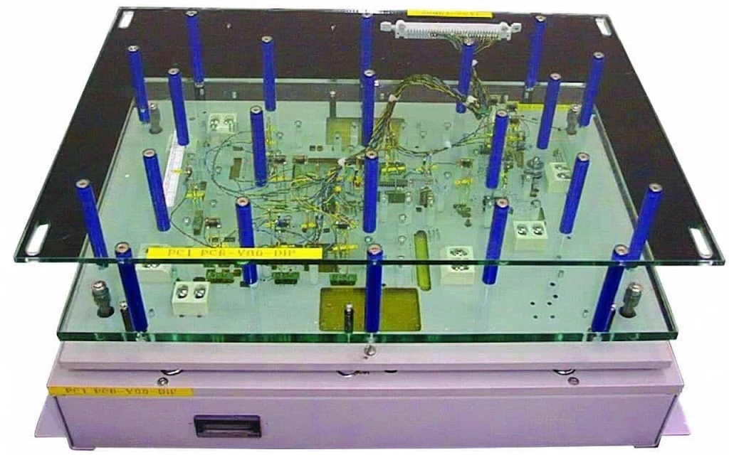
A wave solder fixture (often called a wave solder pallet) is a custom-machined carrier designed to transport Printed Circuit Boards (PCBs) over a molten solder wave while masking sensitive Surface Mount Technology (SMT) components. This wave solder fixture intro covers the essential engineering requirements for shielding bottom-side parts, supporting flexible substrates, and ensuring thermal stability during the 260°C soldering process. By strictly controlling wall thickness and chamfer angles, manufacturers prevent solder defects like shadowing and bridging.
Key Takeaways
- Primary Function: Fixtures shield bottom-side SMT parts (glue-cured) from the wave while exposing Through-Hole Technology (THT) leads for soldering.
- Material Standard: High-quality fixtures use CDM (Composite Delmat Material) or Durostone, capable of withstanding 280°C–300°C for short durations without warping.
- Critical Metric: The minimum wall thickness between a solder pad and the fixture wall must be ≥ 0.50 mm (ideally 1.0 mm) to prevent breakage.
- Clearance Rule: Maintain a 3.0 mm to 5.0 mm clearance around THT pads to allow solder flow and prevent the "shadow effect."
- Validation Tip: Always perform a "fit check" with populated dummy components before the first production run to verify pocket depths.
- Misconception: Thicker fixtures are not always better; a fixture > 10 mm thick may absorb too much heat, causing cold solder joints on the PCB.
- Decision Rule: If the PCB is < 1.0 mm thick or is a Rigid-Flex PCB, a fixture is mandatory to prevent sagging.
What It Really Means (Scope & Boundaries)
In the context of PCB Assembly (PCBA), a wave solder fixture is not just a holder; it is a thermal shield and a mechanical stabilizer. When a board contains a mix of SMT and THT components, the SMT parts on the bottom side (soldering side) must be protected from the molten solder wave, or they will be washed away or shorted.
The scope of a wave solder fixture intro involves understanding three physical boundaries:
- Z-Axis Control: The fixture must hold the PCB flat. For boards thinner than 1.2 mm, gravity and heat will cause sagging. The fixture uses hold-downs to maintain flatness within 0.2 mm.
- Thermal Mass: The fixture material adds thermal mass. If the fixture is too heavy, it steals heat from the THT pins, requiring a hotter wave profile or slower conveyor speed.
- Fluid Dynamics: The fixture walls create turbulence in the solder wave. If the walls are too steep or too close to the pad, the solder cannot flow into the hole (shadowing).
Engineers must balance rigidity with flow. A fixture that is too open risks board warping; a fixture that is too closed risks solder skips.
Metrics That Matter (How to Evaluate It)
To ensure a fixture performs correctly in a Mass Production environment, specific measurable attributes must be verified.
Table 1: Material & Mechanical Properties
| Metric | Acceptable Range | Why It Matters |
|---|---|---|
| Operating Temperature | 260°C (Continuous) / 300°C (Short) | Prevents delamination during the wave cycle. |
| Surface Resistivity | $10^5$ to $10^9$ $\Omega$/sq | Ensures ESD safety; prevents static discharge to sensitive ICs. |
| Flatness Tolerance | $\pm 0.10$ mm over 300 mm | Prevents solder leakage (flooding) onto the masked areas. |
| Life Cycle | > 10,000 cycles | Determines ROI; cheap materials degrade after 500–1,000 cycles. |
| Density | 1.85 – 1.95 g/cm³ | Affects the thermal mass and heat absorption rate. |
| Water Absorption | < 0.20% | Prevents moisture expansion and "popcorning" of the fixture. |
Table 2: Design & Clearance Thresholds
| Feature | Minimum Limit | Recommended | Failure Risk |
|---|---|---|---|
| Wall Thickness (Ribs) | 0.8 mm | 1.5 mm | Walls < 0.8 mm often crack during cleaning or handling. |
| Solder Pad Clearance | 2.0 mm | 4.0 mm | Clearance < 2.0 mm causes "shadowing" (solder skips). |
| Pocket Depth Clearance | Component Height + 0.5 mm | Component Height + 1.0 mm | Insufficient depth crushes SMT capacitors. |
| Chamfer Angle | 30° | 45° | Steep angles block solder flow; 45° promotes smooth flow. |
| PCB Edge Support | 2.0 mm | 3.0 mm | Less than 2.0 mm risks the PCB popping out of the fixture. |
| Hold-Down Pressure | N/A | Spring-loaded | Rigid clamps may warp the board as it expands. |
How to Choose (Selection Guidance by Scenario)
Selecting the right fixture configuration depends on the PCB technology and production volume. Use these decision rules to determine the best approach.
Figure 1: Rigid-Flex PCBs require specialized fixtures to support the flexible sections during soldering.
- If the production volume is < 500 units, choose a universal adjustable pallet or a low-cost FR4 fixture (if thermal tolerance allows).
- If the production volume is > 5,000 units, choose Durostone/CDM material with titanium stiffeners for maximum durability.
- If the PCB is a Flex PCB or Rigid-Flex, choose a fixture with a full-bed support and magnetic hold-downs to keep the flex area flat.
- If the board has heavy components (transformers > 50g), choose a fixture with top-side alignment pins to prevent shifting.
- If the THT components are close to SMT parts (< 3 mm), choose a fixture with titanium inserts (thin walls) rather than standard CDM machining.
- If the PCB thickness is < 1.0 mm, choose a fixture with a top-hat (lid) to sandwich the board and prevent warping.
- If the facility uses aggressive flux (high acidity), choose a Teflon-coated or sealed-surface fixture to resist chemical erosion.
- If Selective Soldering is available, choose to bypass the wave fixture entirely for high-density boards to avoid thermal shock.
- If the board requires Conformal Coating later, choose masking strips on the fixture to keep edge rails clean (though usually handled separately).
- If ESD sensitivity is Class 0 (< 250V), choose a fixture material certified for dissipative properties ($10^6$–$10^9$ $\Omega$).
Implementation Checkpoints (Design to Manufacturing)
A successful wave solder fixture intro requires a disciplined workflow. Follow these 10 checkpoints to move from Gerber data to a production-ready pallet.
Data Analysis (Gerber & BOM):
- Action: Overlay the bottom-side SMT layer with the Drill layer.
- Check: Identify THT pins closer than 3.0 mm to SMT pads.
Component Height Verification:
- Action: Measure the tallest bottom-side component (usually a connector or capacitor).
- Check: Ensure fixture pocket depth is Tallest Component + 0.5 mm.
Thermal Profile Simulation:
- Action: Estimate the added thermal mass of the fixture.
- Check: Verify that the wave contact time will not exceed 5 seconds to achieve barrel fill.
Chamfer Design:
- Action: Apply a 45° chamfer to all solder openings on the solder-flow side.
- Check: Ensure the chamfer does not reduce the supporting wall width below 0.8 mm.
Gas Release Channels:
- Action: Route channels on the underside of the fixture.
- Check: Verify paths allow flux gases to escape, preventing blowholes.
Hold-Down Placement:
- Action: Position rotatable hold-downs on clear PCB areas (no components).
- Check: Ensure hold-downs do not interfere with the wave nozzle or conveyor fingers.
CNC Machining:
- Action: Machine the fixture from ESD-safe composite material.
- Check: Verify dimensional accuracy to ±0.05 mm.
Post-Machining Cleaning:
- Action: Ultrasonic clean to remove dust and oils.
- Check: Surface must be free of debris that could fall into the solder pot.
Fit Check (Dry Run):
- Action: Insert a populated PCB (with SMT) into the fixture.
- Check: No interference; PCB sits flush; hold-downs engage securely.
First Article Inspection (FAI):
- Action: Run one board through the wave.
- Check: Inspect for solder skips (shadowing) and bridging. Verify IPC-A-610 Class 2 or 3 compliance.
Common Mistakes (and the Correct Approach)
Even with a solid design, process failures occur. Here are the most common pitfalls in wave solder fixture engineering.
Mistake 1: Insufficient Wall Thickness
- Impact: Walls between pockets break after 50 thermal cycles.
- Fix: Use titanium inserts for walls thinner than 1.0 mm.
- Verify: Visual inspection for hairline cracks after every 100 cycles.
Mistake 2: Ignoring Thermal Expansion (CTE)
- Impact: PCB bows or snaps out of the fixture at 260°C.
- Fix: Leave 0.2 mm – 0.4 mm gap around the PCB perimeter for expansion.
- Verify: Check if the board floats slightly when cold.
Mistake 3: "Shadowing" Effect
- Impact: Solder fails to reach the pad behind a steep fixture wall.
- Fix: Orient the board so THT rows are parallel to the wave, or increase clearance to 5.0 mm.
- Verify: X-ray or visual check for incomplete barrel fill.
Mistake 4: Flux Trapping
- Impact: Flux residues accumulate in pockets, causing corrosion or fire risk.
- Fix: Design drainage channels and wash fixtures regularly.
- Verify: Inspect pockets for sticky residue daily.
Mistake 5: Over-tight Hold-downs
- Impact: Board warps during cooling; ceramic capacitors crack.
- Fix: Use spring-loaded hold-downs with limited Z-travel.
- Verify: Ensure the board can expand horizontally under the clamp.
Mistake 6: Using Generic FR4 for High Volume
- Impact: Fixture delaminates and loses flatness after 500 cycles.
- Fix: Use CDM/Durostone for volumes > 1,000.
- Verify: Measure fixture flatness monthly.
Mistake 7: Blocking Pre-heat Airflow
- Impact: Top-side of PCB remains cold; poor solder wetting.
- Fix: Add ventilation holes in large solid areas of the fixture.
- Verify: Use a thermal profiler to check top-side preheat temp (target 100°C–120°C).
Mistake 8: Sharp Corners in Pockets
- Impact: Stress concentrators cause fixture cracking.
- Fix: Use a minimum radius of 1.0 mm in all machined corners.
- Verify: Review CNC tool paths.
FAQ (Cost, Lead Time, Materials, Testing, Acceptance Criteria)
1. What is the typical lead time for a custom wave solder fixture? Standard lead time is 3 to 5 working days after Gerber approval. Complex fixtures with titanium inserts or top-hats may require 5 to 7 days. Expedited services can sometimes deliver in 24–48 hours.
2. How much does a wave solder fixture cost? Costs vary by size and complexity.
- Simple FR4 fixture: $150 – $300.
- Standard CDM/Durostone fixture: $350 – $600.
- Complex fixture with titanium inserts: $800+.
3. How do I know when to replace a fixture? Replace the fixture when:
- Wall thickness degrades or chips.
- Flatness deviates by more than 0.2 mm.
- Surface resistivity drifts outside the ESD safe range ($> 10^{11} \Omega$).
- Visible delamination or resin erosion appears.
4. Can I use the same fixture for different PCB revisions? Only if the bottom-side SMT layout and THT locations remain identical. Even a 0.5 mm shift in a capacitor location can cause interference. Universal adjustable pallets exist but offer less protection than custom fixtures.
5. What data is required to design a fixture? Fabricators need:
- Gerber files (Paste, Solder Mask, Drill, Outline layers).
- BOM (to verify component heights).
- XY Centroid file (Pick and Place data).
- A physical sample board (populated) is highly recommended for final fit check.
6. How does the fixture affect the wave solder profile? The fixture absorbs significant heat. You typically need to:
- Increase pre-heat dwell time by 15–30 seconds.
- Increase pot temperature slightly (e.g., from 255°C to 260°C).
- Verify the profile using a profiler mounted on the fixture.
7. What is the difference between a "Selective Wave" fixture and a standard one? A standard fixture exposes all THT parts to a wide wave. A selective wave fixture (used in Selective Soldering) is rarely used; instead, the machine uses a mini-wave nozzle to solder individual points without a fixture. However, "selective wave fixtures" usually refer to pallets that mask 90% of the board for a standard wave machine.
8. How do you validate a fixture before production? Validation steps include:
- Fit Check: Ensure no collision with SMT parts.
- Leak Test: Run through the wave with thermal paper or a dummy board to ensure no solder floods the masked areas.
- ESD Test: Measure surface resistance.
Glossary (Key Terms)
| Term | Definition |
|---|---|
| CDM (Composite Delmat Material) | A fiber-reinforced plastic designed for high-temperature soldering environments; resistant to chemicals and heat. |
| Durostone | A brand name often used generically for heavy-duty glass-fiber reinforced pallet materials. |
| Shadowing | A defect where the fixture wall blocks the flow of solder, leaving a pad unsoldered. |
| Bridging | An unwanted electrical connection between two conductors created by excess solder. |
| Chamfer | An angled cut (usually 45°) on the fixture wall to improve solder flow and reduce turbulence. |
| Hold-down | A mechanical clip or latch used to secure the PCB to the fixture and maintain flatness. |
| Titanium Insert | A metal reinforcement used in fixtures where thin walls (< 1 mm) are required for tight clearance. |
| Flux Trap | A poorly designed pocket where flux accumulates, leading to cleaning issues and potential corrosion. |
| Aspect Ratio | In fixtures, the ratio of the pocket depth to the opening width; high ratios lead to poor soldering. |
| Flooding | When solder flows over the fixture walls onto the protected SMT areas, usually due to warping. |
| Stiffener | A metal bar attached to the fixture edges to prevent bowing over large spans. |
| Thieving Pad | A pad on the PCB (or fixture design feature) intended to draw excess solder away to prevent bridging. |
Conclusion (Next Steps)
Mastering the wave solder fixture intro phase is critical for high-yield assembly. A well-designed fixture protects the PCBA, ensures consistent solder joints, and extends the lifespan of the assembly process. By adhering to the metrics of 1.5 mm wall thickness, 0.5 mm clearance, and rigorous thermal profiling, manufacturers can avoid costly rework.
For complex assemblies involving High Density Interconnect (HDI) or mixed-technology boards, early collaboration with your assembly partner is essential. Ensure your data package includes accurate component heights and clear keep-out zones.
Ready to optimize your wave soldering process? Contact our engineering team for a DFM review or to quote your next custom fixture.