Key Takeaways
Before diving into the technical depths of quantum interconnects, here are the essential points engineering teams must understand.
- Material Matters: Standard gold wire is often unsuitable for superconducting qubits due to residual resistance; aluminum (1% silicon) is the standard for cryogenic environments.
- Inductance is Parasitic: The length and loop height of the wirebond directly add inductance, which can detune the qubit frequency.
- Surface Finish Criticality: Magnetic materials (like standard Nickel in ENIG) destroy qubit coherence; non-magnetic finishes like ENEPIG or Soft Gold are mandatory.
- Mechanical Stress: The interface must survive repeated thermal cycling from room temperature (300K) to milliKelvin (mK) ranges without lifting.
- Frequency Response: The wirebond acts as a discontinuity in the transmission line; keeping bonds short minimizes impedance mismatch.
- Validation: Room temperature continuity testing is insufficient; DC resistance ratios (RRR) and cryogenic pull tests are often required.
What wirebonding for qubit interface really means (scope & boundaries)
Understanding the core requirements of wirebonding for qubit interface begins with acknowledging that standard IPC Class 3 reliability is not enough for quantum applications.
In traditional electronics, wirebonding connects a silicon die to a lead frame or PCB to transmit power and logic signals. In the quantum realm, wirebonding for qubit interface serves a dual purpose: it provides electrical connectivity while maintaining the delicate quantum state (coherence) of the qubit. This interface operates in a regime where single photons matter, and thermal noise must be virtually non-existent.
The scope of this process differs from standard assembly in three ways:
- Thermal Regime: The bond must hold mechanical integrity at near-absolute zero temperatures (10mK to 4K).
- Electromagnetic Environment: The wire loop itself becomes a radiating element. If not controlled, it acts as an antenna, picking up noise or radiating energy that causes decoherence.
- Superconductivity: For superconducting qubits, the wirebond itself must often become superconducting to prevent energy dissipation (heating) at the connection point.
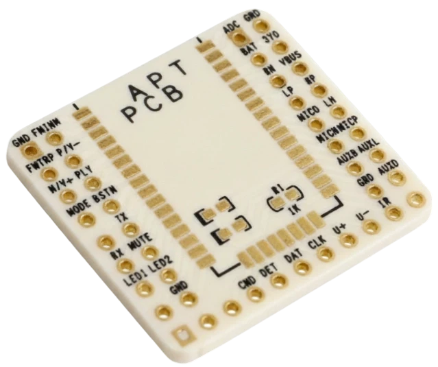
APTPCB (APTPCB PCB Factory) often advises clients that the substrate design (PCB) and the assembly process (wirebonding) cannot be treated separately in quantum applications. The pad geometry on the PCB dictates the bond shape, which in turn dictates the inductance.
wirebonding for qubit interface metrics that matter (how to evaluate quality)
Once the scope is defined, engineers must quantify success using specific metrics that go beyond standard pull strengths.
The following table outlines the critical performance indicators for a high-quality quantum interface.
| Metric | Why it matters | Typical Range / Factor | How to measure |
|---|---|---|---|
| Parasitic Inductance | High inductance alters the resonant frequency of the qubit and limits bandwidth. | 0.5 nH to 2.0 nH (geometry dependent) | VNA (Vector Network Analyzer) or TDR simulation. |
| Bond Shear Strength | Ensures mechanical reliability during thermal contraction/expansion. | > 5 grams (depending on wire diameter) | Dage bond tester (shear test). |
| Critical Current (Ic) | The maximum current the bond can carry without breaking superconductivity. | > 10 mA (application specific) | 4-point probe measurement at cryogenic temps. |
| Impedance Mismatch | Reflections at the bond interface cause signal loss and standing waves. | Target 50 Ohms (VSWR < 1.2) | TDR (Time Domain Reflectometry). |
| Residual Resistance Ratio (RRR) | Indicates the purity of the metal and its performance at low temps. | > 10 for Al wires | Ratio of Resistance at 300K vs. 4K. |
| Loop Height Consistency | Variations in height change inductance, causing qubit frequency spread. | ± 10 µm tolerance | Optical profiling / 3D AOI. |
How to choose wirebonding for qubit interface: selection guidance by scenario (trade-offs)
With the metrics established, the next step is selecting the right bonding strategy based on your specific quantum architecture.
Different qubit modalities (Superconducting, Spin, Trapped Ion) impose different constraints on the wirebonding process.
Scenario 1: Superconducting Transmon Qubits
- Requirement: Zero resistance path and minimal magnetic noise.
- Recommendation: Aluminum Wedge Bonding.
- Trade-off: Aluminum wires are harder to bond to certain gold surfaces than gold wires. You must ensure the PCB surface finish is compatible (e.g., thick soft gold or aluminum pads). Ultrasonic wedge bonding is preferred over thermosonic ball bonding to avoid heating the sensitive Josephson junctions.
Scenario 2: Spin Qubits in Silicon
- Requirement: High-density gate lines, less sensitive to magnetic noise than transmons, but space is tight.
- Recommendation: Gold Ball Bonding (if non-magnetic barrier used).
- Trade-off: Gold is easier to bond and allows for tighter pitch (fine pitch). However, gold is not a superconductor. If the lines carry significant current, heat dissipation becomes a problem.
Scenario 3: High-Frequency Control Lines (4-8 GHz)
- Requirement: Impedance matching is paramount to prevent signal reflection.
- Recommendation: Ribbon Bonding.
- Trade-off: Using a flat ribbon instead of a round wire reduces inductance and improves impedance matching closer to 50 Ohms. The trade-off is that ribbon bonding requires specialized wedge tools and larger bond pads on the High Frequency PCB.
Scenario 4: 3D Integration / Multi-chip Modules
- Requirement: Connecting multiple quantum chips vertically or horizontally.
- Recommendation: Short-loop Wedge Bonding.
- Trade-off: Keeping loops extremely short minimizes inductance but increases mechanical stress during thermal cycling. The CTE (Coefficient of Thermal Expansion) mismatch between the chip and the interposer must be minimal.
Scenario 5: Tuning and Frequency Adjustment
- Requirement: Post-fabrication adjustment of inductance.
- Recommendation: Adaptive Loop Profiling.
- Trade-off: Similar to precision antenna tuning and trimming in RF manufacturing, the shape of the wirebond can be adjusted to "tune" the inductance. This requires highly advanced bonding equipment capable of complex loop profiles, increasing manufacturing cost.
Scenario 6: Rapid Prototyping
- Requirement: Fast turnaround to test chip designs.
- Recommendation: Manual or Semi-Auto Wedge Bonding.
- Trade-off: Manual bonding is slower and less consistent (higher inductance variation) but allows for immediate testing without complex programming. Suitable for proof-of-concept, not production.
wirebonding for qubit interface implementation checkpoints (design to manufacturing)

Selecting the right method is only half the battle; rigorous implementation protocols are required to ensure the interface survives the transition from design to the dilution refrigerator.
Phase 1: PCB/Substrate Design
- Surface Finish Selection: Specify ENEPIG (Electroless Nickel Electroless Palladium Immersion Gold) or Soft Gold. Avoid standard HASL or Immersion Tin. Ensure the Nickel layer is non-magnetic (high phosphorus) if used, or eliminated entirely.
- Pad Geometry: Design pads to accommodate the "foot" of the wedge bond. For ribbon bonding, pads must be rectangular and aligned with the signal path.
- Grounding: Surround signal pads with ground vias (ground-signal-ground configuration) to maintain impedance up to the bond point.
Phase 2: Material Sourcing
- Wire Purity: Source 99.999% (5N) Aluminum or Aluminum-1% Silicon wire. Impurities scatter electrons and break superconductivity.
- Substrate Quality: Use Ceramic PCB (Alumina or Aluminum Nitride) for better thermal matching with silicon chips compared to FR4.
Phase 3: Pre-Bonding Preparation
- Plasma Cleaning: Implement an Argon/Oxygen plasma clean cycle immediately before bonding to remove organic contaminants from pads. This is critical for wedge bonding reliability.
- Bake-out: Remove moisture from the substrate. Moisture trapped in the PCB can outgas in the vacuum chamber or freeze/expand during cooldown, cracking the bond.
Phase 4: Bonding Process
- Parameter Optimization: Perform a DOE (Design of Experiments) for Ultrasonic Power, Time, and Force. The window for quantum chips is narrow—too much power damages the qubit; too little results in lift-offs.
- Loop Control: Program the bonder for "low loop" or "flat loop" profiles to minimize parasitic inductance.
Phase 5: Post-Bond Validation
- Non-Destructive Pull Test: Apply a very light force (e.g., 1g) to ensure no "false bonds" exist.
- Visual Inspection: Check for heel cracks and bond placement accuracy.
- Cryogenic Qualification: Randomly sample units for thermal shock testing (dip in liquid nitrogen) followed by continuity checks.
wirebonding for qubit interface common mistakes (and the correct approach)
Even experienced engineers encounter pitfalls when shifting from classical to quantum interconnects.
Mistake 1: Using Magnetic Underlayers
- The Error: Using standard ENIG (Electroless Nickel Immersion Gold) where the Nickel layer is magnetic.
- The Consequence: The magnetic field from the Nickel disrupts the qubit's spin state or flux, reducing coherence time.
- The Fix: Specify non-magnetic Nickel-Phosphorus or use a direct Gold-on-Copper or Silver finish.
Mistake 2: Ignoring CTE Mismatch
- The Error: Bonding a Silicon chip directly to a standard FR4 board with short, tight wires.
- The Consequence: When cooled to 10mK, FR4 shrinks much more than Silicon. The tension snaps the wires.
- The Fix: Use a CTE-matched interposer or leave a "service loop" (slack) in the wire, though this trades off inductance.
Mistake 3: Over-bonding (Too much force/power)
- The Error: Applying high ultrasonic energy to ensure a strong stick.
- The Consequence: This can create cratering (micro-cracks) in the underlying substrate or damage the delicate Josephson junctions on the chip.
- The Fix: Use the minimum energy required for a reliable bond. Validate with shear testing on dummy samples first.
Mistake 4: Long Wire Loops
- The Error: Allowing large, arching loops for easier bonding clearance.
- The Consequence: Increases inductance significantly ($L \approx 1 \text{nH/mm}$). This acts as a low-pass filter and creates impedance discontinuities.
- The Fix: Keep bonds as short and flat as possible. Place the chip cavity or PCB shelf at the same height as the chip surface (flush mounting).
Mistake 5: Neglecting Oxide Removal on Aluminum
- The Error: Bonding to aluminum pads that have oxidized without proper cleaning.
- The Consequence: High resistance contacts or non-sticking bonds.
- The Fix: Aggressive plasma cleaning or mechanical scrubbing (part of the wedge bonding action) is required to break the oxide layer.
Mistake 6: Assuming Room Temp Tests Equal Cryo Performance
- The Error: Passing a unit based solely on 300K continuity checks.
- The Consequence: Bonds may fail mechanically upon cooling ("open" circuit) or exhibit non-linear resistance.
- The Fix: Perform "cold dip" testing on sample lots.
wirebonding for qubit interface FAQ (cost, lead time, materials, testing, acceptance criteria)
Q: How does wirebonding for qubit interface affect the cost of the PCB assembly? A: It increases cost due to the need for specialized materials (high-purity Al wire), specialized substrates (Ceramic or Rogers), and the lower throughput of precision wedge bonding compared to high-speed ball bonding. Additionally, the NRE (Non-Recurring Engineering) for setting up loop profiles is higher.
Q: What is the typical lead time for substrates suitable for quantum wirebonding? A: Standard FR4 is fast, but quantum-grade substrates like Alumina or high-frequency laminates often have lead times of 3–5 weeks. APTPCB offers expedited services for NPI Assembly to reduce this timeline.
Q: Can we use copper wire instead of aluminum for better conductivity? A: Generally, no. Copper oxidizes rapidly and is harder, requiring higher bonding forces that can damage the chip. Furthermore, Aluminum becomes superconducting at 1.2K, making it a perfect zero-resistance conductor for quantum circuits, whereas copper does not.
Q: What are the acceptance criteria for a quantum wirebond? A: Criteria typically include:
- Shear strength > X grams (based on wire diameter).
- Placement accuracy within ±10µm.
- Loop height variation < 5µm.
- Zero heel cracks visible at 100x magnification.
- DC resistance < 0.5 Ohms (at room temp).
Q: How do you test wirebonds without destroying the qubit? A: We use "witness coupons" or dummy chips bonded with the same parameters for destructive testing (pull/shear). The actual quantum chips undergo 100% visual inspection (AOI) and low-current continuity checks if the design allows.
Q: Why is "antenna tuning and trimming" mentioned in the context of wirebonding? A: While primarily an RF term, the concept applies here. The wire loop acts as an inductor. By precisely adjusting the loop shape (trimming the length/height), engineers can "tune" the impedance of the interconnect to match the transmission line, minimizing signal loss.
Q: Does APTPCB handle the wirebonding or just the PCB fabrication? A: APTPCB provides turnkey solutions. We fabricate the high-performance substrate and can manage the PCBA process, including specialized bonding requirements through our advanced assembly partners.
Resources for wirebonding for qubit interface (related pages and tools)
To further assist in your design process, utilize the following resources available on our platform.
- Substrate Selection: Explore Ceramic PCB Capabilities for cryogenic stability.
- Signal Integrity: Use our Impedance Calculator to design your traces before they reach the wirebond pad.
- Surface Finishes: Read about PCB Surface Finishes to choose the right non-magnetic option.
- Assembly Services: Learn about our Turnkey Assembly for complex, high-mix projects.
wirebonding for qubit interface glossary (key terms)
| Term | Definition |
|---|---|
| Wedge Bonding | A bonding technique using ultrasonic energy and pressure to attach wire; preferred for fine pitch and aluminum wire. |
| Ball Bonding | A technique forming a ball at the wire tip; usually faster but requires heat (thermosonic) and typically uses gold. |
| Superconductivity | A state where a material (like Aluminum at <1.2K) has zero electrical resistance. |
| Qubit (Quantum Bit) | The basic unit of quantum information; highly sensitive to noise and heat. |
| Inductance (Parasitic) | Unwanted inductance added by the wire loop, affecting signal frequency and quality. |
| Cryogenic | Relating to extremely low temperatures (typically below 100K, down to mK range). |
| CTE (Coefficient of Thermal Expansion) | The rate at which a material expands/contracts with temperature changes. Mismatch causes bond failure. |
| ENEPIG | Electroless Nickel Electroless Palladium Immersion Gold; a universal surface finish good for wirebonding. |
| Skin Effect | The tendency of high-frequency current to flow near the surface of the conductor; relevant for microwave control lines. |
| Josephson Junction | A key component of superconducting qubits; extremely sensitive to electrostatic discharge and heat. |
| Interposer | An intermediate layer (silicon or ceramic) used to route signals between the chip and the main PCB. |
| Heel Crack | A fracture at the point where the wire transitions from the bond pad to the loop; a common failure mode. |
Conclusion (next steps)
Mastering wirebonding for qubit interface is about managing the intersection of mechanical robustness, cryogenic physics, and microwave engineering. It requires moving away from standard "continuity-only" mindsets and adopting a rigorous approach to material purity, loop geometry, and surface finish.
If you are ready to move your quantum processor or control electronics from design to fabrication, ensure your manufacturing partner understands these unique constraints.
When requesting a quote from APTPCB, please provide:
- Gerber Files: With clear indications of bond pad locations.
- Stackup Details: Including specific dielectric materials (e.g., Rogers, Ceramic).
- Surface Finish Specs: Explicitly state "Non-magnetic" if required.
- Wirebond Diagram: specifying target loop heights and wire material (Al vs. Au).
- Operating Temperature: (e.g., 4K, 10mK) so we can advise on CTE risks.
Reliable quantum hardware starts with a reliable interface. Contact us today to review your design for manufacturability.