
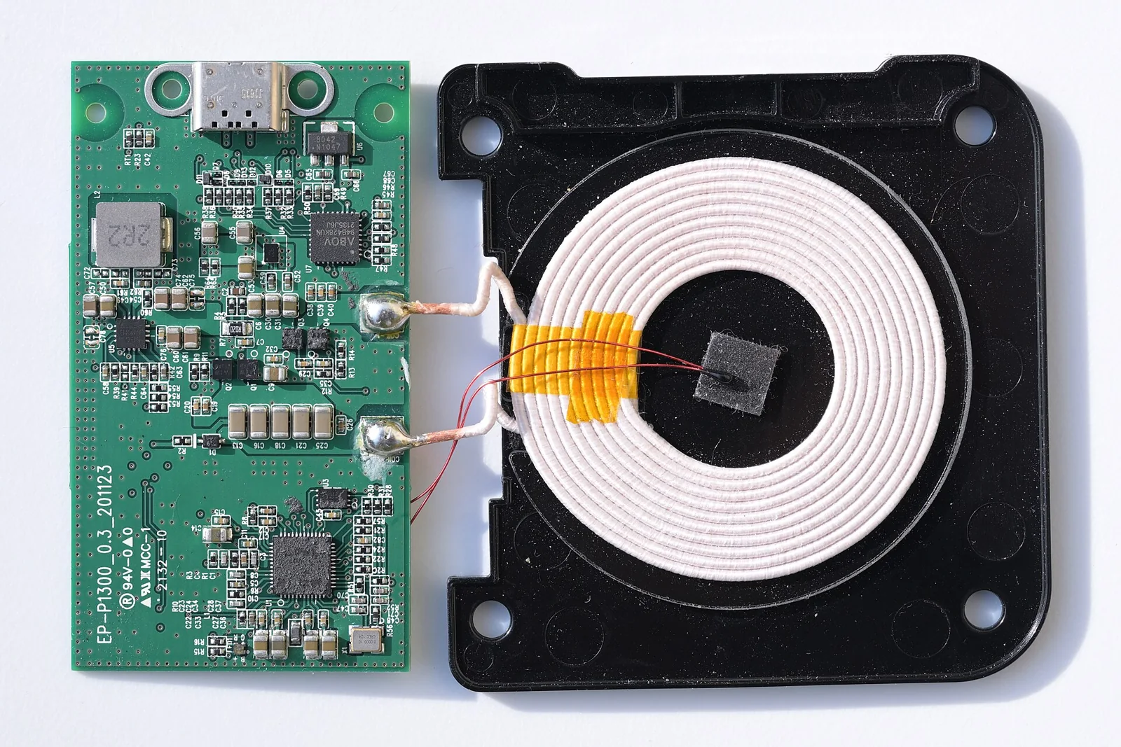
- A wireless charger PCB should be reviewed as a coupled coil-power-thermal subassembly, not as a generic switching board, because its hardest constraints sit in the small zone directly under the coil.
- The first board-level question is whether the coil, ferrite shield, and the copper underneath form a stable magnetic and thermal interface that survives assembly and sustained operation.
- A board can power up cleanly on the bench while the real failure driver is heat and radiated noise concentrated under the coil where there is almost no airflow.
- The coil drive, switching power stage, control, and EMI return paths each carry a different burden, and treating the board as one flat plane is what makes the coupling region misbehave.
- Keep the review at the board boundary. It does not claim Qi interoperability, EMC pass results, or fixed efficiency figures.
Quick Answer A
wireless charger PCBis best reviewed as a board that has to drive a coil, move switching heat out of a confined zone, and contain radiated noise while the coil and ferrite sit directly on top of the power copper. The practical release question is not justDoes the coil energize?It isDoes the coil interface stay thermally and electromagnetically stable after the ferrite, shield, and enclosure are all stacked on the board and the charger runs under sustained load?Application context starts at Power & Energy PCB.
Table of Contents
- What a wireless charger PCB has to balance
- The physical boundary: coil, ferrite, and the board underneath
- Power-stage and EMI layout decisions
- Release implications: what to confirm before the build
- FAQ
- Public references
- Author and review information
What a wireless charger PCB has to balance
Start with the coupling region, not with a power-profile label. An inductive charger board, whether a Qi-class consumer pad or an automotive cradle, is a set of regions that fight each other for the same small footprint. The coil wants clean magnetic space, the power stage wants copper and heat exit, and the control and EMI returns want quiet reference. The board review has to keep those demands distinct instead of averaging them into one plane.
| Review region | What to confirm | Why it matters |
|---|---|---|
| Coil interface | The transmit coil, ferrite shield, and the copper directly beneath form a defined magnetic and mechanical stack with no stray conductive loops in the field | Eddy currents and field distortion start in the layer right under the coil, not in the schematic |
| Power and switching stage | The bridge or half-bridge drive, gate loops, and resonant tank components sit in a compact, low-inductance partition | Switching loops that sprawl become both a heat source and a radiator under the coil |
| Thermal zone under the coil | Heat from the power devices and coil drive has a real exit path despite the ferrite and enclosure sitting on top | The hottest region is the one with the least airflow, which a bench power-on rarely exposes |
| EMI and control returns | Sense lines, communication demod, and control reference are kept off the high di/dt switching returns | Noise coupled into control corrupts the regulation loop and the EMI profile together |
For stackup and construction discussion, the closest support page is PCB Stack-Up. For application context around power hardware, the useful landing pages are Power & Energy PCB and Automotive Electronics PCB.
The physical boundary: coil, ferrite, and the board underneath
The defining feature of a wireless charger board is that an active magnetic component is mounted directly over the copper. That single fact reshapes the whole review. The coil produces a strong alternating field, the ferrite sheet shapes and shields it, and whatever copper sits in that field has to be planned, not left as default pour.
At the board boundary, three things have to be reviewed together in this region:
- the keep-out under and around the coil, so that solid copper planes, vias, and traces do not form closed loops that the field drives into eddy heating
- the ferrite-to-board contact, so the shield seats flat and the magnetic return stays defined rather than leaking into nearby copper or the enclosure
- the mechanical stack, because the coil, ferrite, any thermal pad, and the enclosure lid all press down on the same area and decide how much of the planned heat path is real after assembly
This is also where the primary risk chain begins. The switching power stage and the coil drive both dissipate energy as heat, and both radiate, and they do it directly under the coil and ferrite. That places thermal rise and radiated noise together in a zone that has almost no airflow because the coil, shield, and housing cap it. On the bench, a short power-on looks fine: nothing is saturated yet, the control loop locks, and early electrical checks pass. The trouble appears later. Under sustained charging the capped zone heats steadily, the operating point drifts, and the device may derate or trip thermally, while the same confined switching region keeps radiating into a now warmer, less stable layout. The visible result in the field is surface heating under continuous use or EMI-control behavior that the original bench session never reproduced.
The board-level lesson is that the coil interface is a thermal and electromagnetic problem before it is an efficiency number. If the copper under the coil, the ferrite seating, and the heat exit are reviewed as one stack, the confined zone stays predictable. If they are reviewed separately, the board can pass static checks while the coupling region is already preparing to overheat or misbehave under load.
Power-stage and EMI layout decisions
The power stage is the engine and, in this board class, also the dominant noise source sitting in the worst possible place. The drive bridge, gate loops, and resonant tank carry high di/dt current at the switching rate set by the design and the applicable standard. Every one of those loops is an antenna and a heat source, so the layout review treats loop area as the primary control.
Practical board-level decisions that carry the most weight:
- Keep the switching loops tight. The bridge devices, their decoupling, and the resonant tank should form the smallest practical current loop. Compact loops radiate less and concentrate less stray heating into the coil zone.
- Define the high-current return deliberately. A clear, low-impedance return for the coil drive keeps the switching current off shared planes and away from sense and communication nodes. This is where copper weight and routing choices matter; heavier copper for the drive path is discussed under Heavy Copper PCB.
- Separate the control and demod reference. Communication demodulation and current or voltage sensing read small signals. Routing them across the switching return is how the regulation loop and the EMI signature degrade at the same time.
- Plan the heat exit before placement is frozen. Because the coil and ferrite cap the power stage, the exit path has to go sideways into copper and down into the stack rather than up. For boards that lean on the substrate to spread heat, the relevant construction options are High Thermal PCB and Metal Core PCB.
- Treat the shield and ground as one system. The ferrite shapes the field, but the board ground and any EMI shielding decide where the return and common-mode currents actually flow. Reviewing them together keeps the radiated profile from shifting once the enclosure is added.
The aim of the review is not to predict an EMC result. Qi and the WPC ecosystem define the operating identity of the link, and the applicable standard sets the frequency band and behavior. The board review confirms that the layout gives that link a tight, well-referenced, thermally honest home so the design has a chance to behave as intended.
Release implications: what to confirm before the build
Use a staged board review instead of asking a single bench power-on to stand in for sustained-load behavior. The checklist below stays at the board boundary.
| Review question | What to look for | Why it is a release issue |
|---|---|---|
| Is the copper under the coil planned, not default? | Keep-outs and the absence of closed conductive loops in the coil field are explicit in the layout | Eddy heating and field distortion originate in this layer and rarely show on a schematic check |
| Is the heat exit real after the stack is assembled? | The path from power devices and coil drive into copper and the substrate survives the ferrite, pad, and enclosure load | The capped zone has the least airflow, so a nominal thermal plan can quietly disappear after assembly |
| Are switching loops tight and returns defined? | Drive loop area is minimized and the high-current return is isolated from sense and comms | Sprawling loops radiate and heat the coil zone at the same time |
| Is the control reference protected? | Demod and sense routing is kept off the switching return and on a quiet reference | Noise into control degrades regulation and the EMI profile together |
| Is the validation language still at board level? | Review stays on DFM, stackup intent, coil and ferrite seating, heat path, and test planning | A board release should not be read as Qi interoperability or EMC certification |
If the release package still needs stackup cleanup or manufacturing-note alignment, the companion resource is DFM Guidelines. For PCBA-side validation language, the closest pages are Testing & Quality and, for functional verification of the powered board, FCT Test.
The most useful inputs for this review are fabrication data with stackup intent, placement that makes the coil, ferrite, power, and control zones easy to read, BOM context for the drive devices and resonant components, and mechanical references for the coil, shield, thermal pad, and enclosure touch points. With those in hand, the board team can comment on the real wireless-charging release problem rather than on broad manufacturability. When the design is ready for a manufacturing review, the intake path is the wireless charger PCB review request.
FAQ
Does a wireless charger PCB article prove Qi interoperability?
No. A board-level review explains how to plan the coil interface, power stage, and thermal zone. It does not prove Qi or WPC interoperability, which is established through the applicable certification process, not a layout review.
Why is the copper under the coil treated as a special region?
Because that copper sits inside a strong alternating field. Solid planes, vias, or traces that form closed loops there can carry induced eddy currents, which produce localized heating and distort the field the link depends on.
Can a board pass a bench power-on and still fail under sustained charging?
Yes. A short power-on may not reveal the confined heating and radiated-noise behavior that build up only after the coil, ferrite, and enclosure are stacked and the charger runs continuously with little airflow.
Why review the power stage and EMI together?
The switching loops are both the dominant heat source and the dominant radiator, and they sit directly under the coil. Tightening loop area and defining the return path improves the thermal and EMI picture at the same time.
Should the whole board use one thermal and grounding strategy?
Not usually. The coil interface, power stage, and control area each need a different priority. Treating the board as one flat plane tends to hide the constraints that concentrate in the coupling region.
What is the most useful package to send before release?
The strongest package combines fabrication data with stackup intent, placement that exposes the coil and power zones, BOM context for the drive and resonant parts, and mechanical references for the coil, ferrite, thermal pad, and enclosure interfaces.
Public references
Power & Energy PCB Application-page context for charger, converter, and power-board manufacturing scope.
Automotive Electronics PCB Application-page context for in-vehicle power and charging hardware discussions.
PCB Stack-Up Support-page context for stackup definition and controlled construction planning.
High Thermal PCB Support-page context for substrate-led heat spreading in confined power zones.
DFM Guidelines Support-page context for manufacturing review intake and pre-release clarification.
Author and review information
- Author: APTPCB editorial team
- Technical review: Power electronics PCB engineering review team
- Review scope: Board-level coil interface, power-stage EMI layout, thermal zone under the coil, manufacturability, and release-boundary consistency