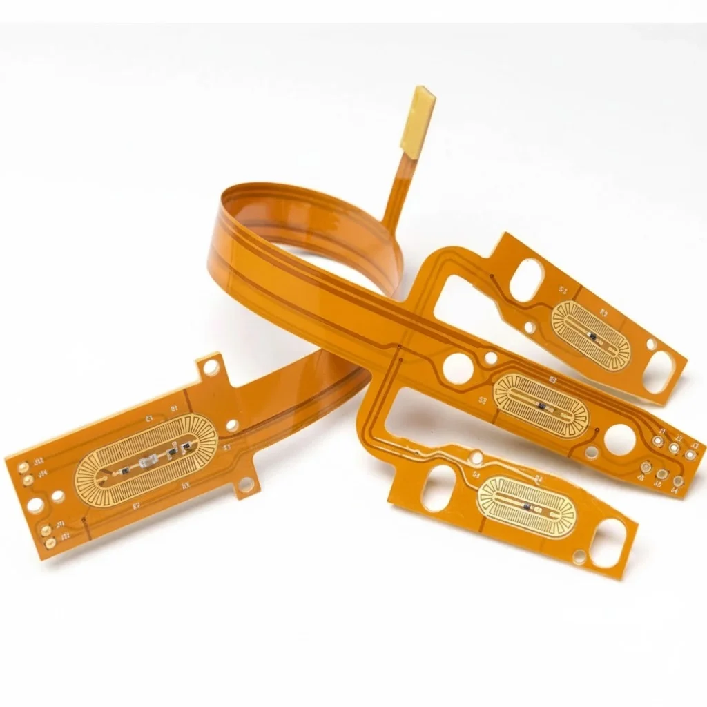
Definition, scope, and who this guide is for
A Wireless PLC PCB represents the convergence of rugged industrial control logic with modern RF connectivity. Unlike traditional Programmable Logic Controllers (PLCs) that rely exclusively on hardwired Ethernet, RS-485, or fieldbus connections, these boards integrate wireless modules (Wi-Fi, Bluetooth, LoRaWAN, 5G/LTE, or Zigbee) directly onto the substrate. This integration allows for seamless data transmission in Cloud PLC PCB architectures and enables remote monitoring in hard-to-reach locations. However, combining high-speed digital switching, high-voltage relay control, and sensitive RF signals on a single board introduces complex manufacturing challenges regarding signal integrity and electromagnetic compatibility (EMC).
This playbook is designed for Senior Electrical Engineers, Procurement Leads, and Product Managers responsible for sourcing high-reliability PCBs for industrial automation. It moves beyond basic fabrication notes to address the specific risks of wireless integration in industrial environments. Whether you are designing a Compact PLC PCB for a tight enclosure or a Distributed PLC PCB system for a sprawling factory floor, the manufacturing quality of the bare board dictates the reliability of the wireless link.
At APTPCB (APTPCB PCB Factory), we see many designs fail not because of bad logic, but because the physical board layout and material stackup could not support the RF requirements in a noisy industrial environment. This guide provides the specifications, risk mitigation strategies, and validation steps necessary to procure a Wireless PLC PCB that performs reliably in the field.
When to use Wireless Programmable Logic Controller (PLC) PCB (and when a standard approach is better)
Understanding the physical constraints of your deployment environment determines whether a wireless-integrated board is the correct engineering choice or if a standard wired solution is safer.
Use a Wireless PLC PCB when:
- Retrofitting Legacy Plants: You need to add smart control to older machinery where running new conduit or cabling is cost-prohibitive or physically impossible.
- Mobile Robotics (AGVs/AMRs): The controller is mounted on a moving platform (Automated Guided Vehicles) where tethered connections are impossible, requiring an
Edge PLC PCBcapable of real-time wireless communication. - Remote/Distributed Assets: The equipment is located in outdoor cabinets, pipelines, or agricultural settings where cellular (LTE/NB-IoT) is the only connectivity option.
- IIoT Data Aggregation: The PLC acts as a gateway, collecting sensor data via Bluetooth/Zigbee and uploading it to the cloud via Wi-Fi, necessitating a
Cloud PLC PCBarchitecture.
Stick to Standard Wired PLC PCB when:
- Ultra-Low Latency is Critical: If the application requires sub-millisecond synchronization (e.g., multi-axis motion control), wireless packet loss or jitter is unacceptable.
- High EMI Environments: In close proximity to massive VFDs (Variable Frequency Drives) or arc welding equipment, wireless signals may be swamped by noise regardless of shielding.
- Security Constraints: Air-gapped facilities (nuclear, defense) often strictly prohibit wireless interfaces at the hardware level.
Wireless Programmable Logic Controller (PLC) PCB specifications (materials, stackup, tolerances)
Once the decision to go wireless is made, you must translate performance goals into concrete fabrication data to ensure the board supports RF fidelity.
- Base Material (Laminate):
- Standard: High-Tg FR4 (Tg > 170°C) for general durability.
- RF Critical: For frequencies > 2.4GHz or long trace runs, specify low-loss materials (e.g., Panasonic Megtron 6 or Rogers RO4350B) for the RF layers, or use a Hybrid Stackup (FR4 + Rogers).
- Impedance Control:
- RF Traces: 50Ω ±5% (strictly controlled) for antenna feedlines.
- Differential Pairs: 90Ω or 100Ω ±10% for USB, Ethernet, or MIPI interfaces connecting the wireless module.
- Layer Stackup:
- Minimum: 4-layer board is the absolute minimum to provide a solid ground plane for the antenna.
- Recommended: 6-8 layers for
Compact PLC PCBdesigns to isolate noisy power planes from sensitive RF layers.
- Surface Finish:
- Requirement: ENIG (Electroless Nickel Immersion Gold) or ENEPIG.
- Reason: Provides a flat surface for fine-pitch RF modules and prevents oxidation that affects high-frequency skin effect conductivity.
- Copper Weight:
- Power Section: 2oz or 3oz for relay driving and power supply inputs.
- RF/Logic Section: 0.5oz or 1oz to allow for fine line etching (trace width/spacing < 5 mil).
- Vias and Plating:
- Stitching Vias: Specify "via fencing" or "shielding vias" along RF traces (spaced < λ/20 of the operating frequency).
- Filled Vias: VIPPO (Via-in-Pad Plated Over) may be required for BGA wireless modules to fan out signals in tight spaces.
- Solder Mask:
- Color: Green is standard, but Matte Black or Blue is often used for optical inspection contrast.
- Clearance: Strict mask expansion rules (e.g., 1:1 or +2mil) to prevent mask encroaching on RF pads.
- Dimensional Tolerances:
- Outline: ±0.10mm (critical if the PCB antenna must align with a housing window).
- Drill Position: ±0.075mm to ensure via fencing does not short to the trace.
Wireless Programmable Logic Controller (PLC) PCB manufacturing risks (root causes and prevention)
Defining specs is step one; understanding where Wireless PLC PCB production typically fails allows you to preemptively address issues during the NPI phase.
- Risk: Impedance Mismatch causing Signal Loss
- Why: Fabricator variation in etching or prepreg thickness changes the trace impedance.
- Detection: TDR (Time Domain Reflectometry) coupons fail or show high variance.
- Prevention: Specify "Impedance Control" clearly in Gerber files and request a TDR report for every batch.
- Risk: EMI Self-Interference (Desense)
- Why: Noisy DC-DC converters or high-speed clocks on the PLC couple noise onto the wireless antenna.
- Detection: Poor wireless range or high packet error rate during active processing.
- Prevention: Use shielding cans over power circuits; separate RF and Power grounds with a "star ground" or ferrite bead bridge.
- Risk: Thermal Throttling of RF Modules
- Why: RF amplifiers generate heat; if the PCB cannot dissipate it, the module throttles power.
- Detection: Throughput drops after 10-15 minutes of operation.
- Prevention: Design thermal via arrays under the RF module belly pad; use high-thermal-conductivity FR4.
- Risk: Warp and Twist affecting Antenna Tuning
- Why: Unbalanced copper distribution (heavy power planes vs. sparse RF layers) causes bowing during reflow.
- Detection: Board does not sit flat in the fixture; antenna geometry is distorted.
- Prevention: Copper thieving (hatching) on empty layer areas to balance stress; use high-Tg materials.
- Risk: Passive Intermodulation (PIM)
- Why: Poor quality copper surface or oxidation creates non-linear junctions.
- Detection: Unexplained noise floor increase in the RF band.
- Prevention: Use high-quality ENIG finish; ensure clean etching processes.
- Risk: CAF (Conductive Anodic Filament) Growth
- Why: High voltage (PLC I/O) + Humidity + tight spacing leads to internal shorts over time.
- Detection: Field failure after months of operation.
- Prevention: Use CAF-resistant materials; maintain sufficient clearance between HV and LV sections.
- Risk: Connector Shear under Vibration
- Why: Heavy SMA/U.FL connectors vibrate loose in industrial settings.
- Detection: Intermittent signal loss during vibration testing.
- Prevention: Add epoxy staking or mechanical support holes for RF connectors.
- Risk: Inconsistent Dielectric Constant (Dk)
- Why: Supplier swaps laminate brands between batches without notice.
- Detection: RF center frequency shifts between production lots.
- Prevention: Lock the specific laminate brand and series (e.g., "Isola 370HR only") in the fabrication drawing.
Wireless Programmable Logic Controller (PLC) PCB validation and acceptance (tests and pass criteria)

To ensure your Wireless PLC PCB functions correctly in a Distributed PLC PCB network, you must enforce a rigorous testing regime before accepting the shipment.
- Objective: Verify Impedance Control
- Method: Time Domain Reflectometry (TDR) on test coupons and actual boards (random sampling).
- Criteria: Measured impedance must be within ±5% (or ±10% as specified) of target.
- Objective: Verify Layer Stackup & Material
- Method: Microsection analysis (cross-section) on one board per lot.
- Criteria: Dielectric thicknesses match stackup drawing; copper plating thickness meets IPC Class 2 or 3.
- Objective: Thermal Stress Resistance
- Method: Solder float test (288°C for 10 seconds) or multiple reflow simulations.
- Criteria: No delamination, blistering, or measles; via connectivity remains intact.
- Objective: Surface Finish Quality
- Method: X-Ray Fluorescence (XRF) for gold/nickel thickness; visual inspection for oxidation.
- Criteria: Gold thickness 2-5µin (for ENIG); uniform coverage; no "black pad" defect.
- Objective: Electrical Continuity & Isolation
- Method: 100% Flying Probe or Bed of Nails electrical test.
- Criteria: 100% pass; no opens or shorts; isolation resistance > 10MΩ (or higher for HV sections).
- Objective: RF Shielding Effectiveness (PCBA level)
- Method: Near-field probe scanning over the shield cans and trace boundaries.
- Criteria: Noise leakage below defined threshold (e.g., -80dBm) at operating frequencies.
- Objective: Cleanliness (Ionic Contamination)
- Method: ROSE testing (Resistivity of Solvent Extract).
- Criteria: Contamination < 1.56 µg/cm² NaCl equivalent (crucial for RF and HV reliability).
- Objective: Dimensional Accuracy
- Method: CMM (Coordinate Measuring Machine) or optical measurement.
- Criteria: Outline and mounting holes within ±0.1mm; critical antenna features within ±0.05mm.
Wireless Programmable Logic Controller (PLC) PCB supplier qualification checklist (RFQ, audit, traceability)
When selecting a partner for Wireless PLC PCB manufacturing, use this checklist to vet their capabilities. A generic board house may not understand the nuances of RF integration.
Group 1: RFQ Inputs (What you must provide)
- Complete Gerber files (RS-274X or X2) with clear layer naming.
- Stackup drawing specifying dielectric constant (Dk) and Loss Tangent (Df) requirements.
- Impedance table linking trace widths/layers to target ohms.
- Drill chart distinguishing between plated and non-plated holes.
- "Do Not X-Out" requirement for panelized arrays (if automated assembly is used).
- Material datasheet callout (e.g., "Panasonic Megtron 6 or equivalent approved by engineering").
- Surface finish requirement (ENIG preferred for RF).
- IPC Class requirement (Class 2 standard, Class 3 for critical industrial/aerospace).
Group 2: Capability Proof (What they must demonstrate)
- Do they have in-house TDR testing equipment? (Ask for a sample report).
- Can they handle hybrid stackups (e.g., FR4 + Rogers bonded together)?
- What is their minimum trace width/spacing for impedance controlled lines? (3/3 mil or 4/4 mil is typical).
- Do they have experience with edge plating or castellated holes (often used for RF modules)?
- Can they perform back-drilling to remove via stubs (critical for high-speed signals)?
- What is their registration tolerance for layer-to-layer alignment?
Group 3: Quality System & Traceability
- Are they ISO 9001 and UL certified?
- Do they have a specific workflow for "RF/High-Frequency" products?
- Can they provide material certificates of compliance (CoC) from the laminate manufacturer?
- Do they use Automated Optical Inspection (AOI) on inner layers before lamination?
- How do they handle X-out panels? (Ensure they mark them clearly).
Group 4: Change Control & Delivery
- Will they notify you before changing laminate suppliers or solder mask brands?
- Do they offer DFM (Design for Manufacturing) review specifically for RF structures?
- What is the standard lead time for complex impedance-controlled boards?
- Do they have a local support team or engineering interface?
How to choose Wireless Programmable Logic Controller (PLC) PCB (trade-offs and decision rules)
Designing a Wireless PLC PCB involves balancing performance, size, and cost. Here is how to navigate common trade-offs.
- Integrated PCB Antenna vs. External Connector:
- If you prioritize cost and compactness: Choose an Integrated PCB Trace Antenna. It’s free (just copper) and fits inside the case.
- If you prioritize range and metal enclosure mounting: Choose an External Connector (SMA/RP-SMA). PCB antennas detune inside metal boxes; external antennas solve this.
- Hybrid Material vs. All-FR4:
- If you prioritize signal integrity > 2.4GHz: Choose Hybrid Material (Rogers + FR4). It reduces signal loss significantly.
- If you prioritize cost and operate at standard Wi-Fi/BT: Choose High-Performance FR4. Modern FR4 is often "good enough" for short-range 2.4GHz links.
- Module vs. Chip-Down Design:
- If you prioritize time-to-market and certification: Choose a Pre-certified Wireless Module. You avoid expensive FCC/CE RF certification.
- If you prioritize unit cost at high volume (>50k units): Choose a Chip-Down Design. It is cheaper per unit but requires complex RF design and certification.
- HDI (High Density Interconnect) vs. Through-Hole:
- If you prioritize miniaturization (Compact PLC): Choose HDI (Blind/Buried Vias). Essential for routing BGA wireless chips.
- If you prioritize lower board cost: Choose Standard Through-Hole. Stick to larger modules that don't require micro-vias.
- Shielding Cans vs. Exposed RF:
- If you prioritize reliability in noisy environments: Choose Shielding Cans. They are mandatory for industrial PLCs to pass EMC testing.
- If you prioritize lowest BOM cost: Skip the can, but risk failing EMC or suffering from desense.
Wireless Programmable Logic Controller (PLC) PCB FAQ (cost, lead time, Design for Manufacturability (DFM) files, stackup, impedance, Inconsistent Dielectric Constant (DK)/and Loss Tangent (DF))
Q: Can I use standard FR4 for a 5GHz Wireless PLC PCB?
- Standard FR4 has high signal loss at 5GHz. For short traces (<1 inch), it might work, but for longer runs or critical performance, use a mid-loss or low-loss material like Isola FR408HR or Megtron.
Q: How do I ground the RF section on a PLC PCB?
- Use a solid ground plane immediately below the RF layer. Stitch the ground planes together with vias every λ/20. Keep the RF ground separate from the noisy relay/power ground, connecting them at a single point (star ground).
Q: What is the best surface finish for Wireless PLCs?
- ENIG (Electroless Nickel Immersion Gold) is the industry standard. It provides a flat surface for module soldering and does not suffer from the skin-effect losses associated with HASL (which is uneven) or OSP (which oxidizes).
Q: How does the enclosure affect the PCB design?
- If the PLC uses a plastic case, the PCB antenna can radiate through it. If it uses a metal case (common in industrial), you must use an external antenna connector or route the antenna to a plastic window.
Q: Why is impedance control critical for Wireless PLCs?
- RF energy reflects back if the trace impedance doesn't match the source (50Ω). This reflection causes signal loss (VSWR) and can damage the RF amplifier or corrupt data packets.
Q: What is "via fencing" and do I need it?
- Via fencing is a row of ground vias placed along the edges of an RF trace (Coplanar Waveguide). Yes, you need it to shield the RF signal from internal board noise and prevent crosstalk.
Q: Can APTPCB manufacture hybrid stackups for RF?
- Yes, APTPCB specializes in hybrid laminations, combining cost-effective FR4 with high-performance RF materials to balance cost and performance.
Q: What is the risk of using HASL finish for RF boards?
- HASL leaves an uneven surface, making it hard to solder fine-pitch RF modules. Furthermore, the solder thickness varies, slightly altering the impedance of the traces.
Resources for Wireless Programmable Logic Controller (PLC) PCB (related pages and tools)
- Industrial Control PCB Manufacturing – Deep dive into the specific reliability standards required for industrial automation boards.
- High Frequency PCB Capabilities – Learn about the materials and processes APTPCB uses for RF and microwave applications.
- HDI PCB Technology – Essential reading if you are designing a
Compact PLC PCBrequiring micro-vias and high-density routing. - Turnkey PCB Assembly Services – How to move from bare board fabrication to fully assembled wireless units with one partner.
- DFM Guidelines – Download our design rules to ensure your wireless layout is manufacturable before you quote.
Request a quote for Wireless Programmable Logic Controller (PLC) PCB (Design for Manufacturability (DFM) review + pricing)
Ready to move your Wireless PLC PCB from design to production? Get a comprehensive DFM review and accurate pricing from APTPCB to ensure your RF performance meets industrial standards.
What to prepare for your quote:
- Gerber Files: RS-274X or ODB++ format.
- Fabrication Drawing: clearly marking impedance lines, stackup, and material requirements.
- BOM (Bill of Materials): if you require PCBA services.
- Volume: Prototype quantity vs. Mass production targets.
Click here to Request a Quote & DFM Review – Our engineering team will review your stackup for RF integrity and manufacturability.
Conclusion (next steps)
A successful Wireless PLC PCB is more than just a standard controller with a Wi-Fi chip attached; it is a precision-engineered component that must balance high-voltage industrial control with sensitive RF communication. By defining strict material specifications, validating impedance control, and selecting a supplier who understands the nuances of hybrid stackups and shielding, you can deploy Cloud PLC PCB and Edge PLC PCB solutions that survive the harshest factory environments. Follow the validation steps and checklist in this guide to minimize risk and ensure your product scales without connectivity failures.