Ensuring long-term reliability in Ball Grid Array (BGA) assembly requires rigorous non-destructive testing, specifically focusing on x-ray criteria for bga voiding and head-in-pillow (HiP). Unlike visible solder joints, BGA connections are hidden beneath the component body, rendering standard optical inspection methods ineffective. For engineers and quality managers at APTPCB (APTPCB PCB Factory), understanding the precise pass/fail limits defined by IPC standards is critical for preventing field failures caused by thermal cycling fatigue or intermittent electrical contact. This guide details the specific X-ray signatures, measurement thresholds, and process controls necessary to validate BGA integrity.
Quick Answer (30 seconds)
For reliable BGA assembly, the x-ray criteria for bga voiding and head-in-pillow generally follow IPC-7095 and IPC-A-610 standards.
- Voiding Limits: For IPC Class 2 and Class 3, the total void area within a single solder ball should not exceed 25% of the total ball area.
- Head-in-Pillow (HiP): This is a "process indicator" and is generally not acceptable. It appears as a distinct separation or lack of coalescence between the solder ball and the paste, often resembling a ball resting on a pillow.
- Detection: Voiding is visible in 2D transmission X-ray. HiP often requires angled 2D X-ray (2.5D) or 3D Laminography (CT) because the vertical overlap can mask the defect in a top-down view.
- Critical Location: Voids located at the interface of the solder ball and the component pad (interfacial voids) are more critical and often grounds for rejection regardless of size due to crack propagation risks.
- Validation: Automated X-ray Inspection (AXI) systems must be calibrated to distinguish between benign macro-voids and critical planar micro-voids.
When x-ray criteria for bga voiding and head-in-pillow applies (and when it doesn’t)
Understanding the scope of inspection ensures resources are focused on critical reliability risks rather than cosmetic anomalies.
When these criteria apply:
- BGA and CSP Assembly: Any component where solder joints are obscured by the package body requires X-ray validation against these criteria.
- High-Reliability Products: Automotive, aerospace, and medical devices (IPC Class 3) where thermal cycling can cause voids to coalesce into cracks.
- Process Validation: During the "First Article Inspection" (FAI) phase to tune the reflow profile.
- Troubleshooting Intermittent Failures: When a board passes electrical test but fails under vibration or thermal stress.
- New Package Introduction: When introducing QFNs or LGAs with large thermal pads, where voiding rules differ slightly but the physics remain similar.
When these criteria do not apply (or differ):
- Standard Through-Hole Components: While X-ray can check barrel fill, the voiding criteria for BGAs do not directly translate to wave-soldered joints.
- Visible Gull-Wing Leads: Standard
aoi inspectionis preferred here; X-ray is overkill unless checking for heel fillets. - Thermal Ground Pads (QFN/LGA): Voiding limits for large thermal planes are often looser (up to 50% in some specific customer agreements) compared to signal BGA balls.
- Underfill Applications: Once underfill is applied, X-ray contrast changes, and void detection becomes more complex; criteria must be applied before underfill dispensing.
- Cosmetic Surface Blemishes: X-ray looks through the part; surface scratches on the package body are irrelevant to this specific criteria set.
Rules & specifications
The following table outlines the specific technical parameters used to evaluate BGA integrity. These rules translate the general x-ray criteria for bga voiding and head-in-pillow into measurable data points.
| Rule / Parameter | Recommended Value/Range | Why it matters | How to verify | If ignored |
|---|---|---|---|---|
| Total Void Percentage | < 25% of X-ray image area (IPC Class 2/3) | Large voids reduce thermal and electrical conductivity and weaken mechanical strength. | AXI software area calculation algorithm. | Joint fracture during thermal cycling. |
| Largest Single Void | < 20% of ball area | A single large bubble creates a significant stress concentration point. | Measure diameter of largest low-density region. | Immediate mechanical failure under shock. |
| Head-in-Pillow (HiP) Signature | 0% (Reject) | Indicates no metallurgical bond; the joint is held only by flux residue or mechanical pressure. | Angled X-ray (45-70°) or 3D CT slice analysis. | Intermittent open circuits in the field. |
| Solder Ball Diameter | ±15% of nominal datasheet value | Variations indicate stretching (warpage) or squashing (heavy components). | Comparative measurement against reference balls. | Open joints or short circuits. |
| Solder Bridge / Short | 0 (None allowed) | Direct electrical failure. | High-density link between adjacent pads on X-ray. | Immediate functional failure (short circuit). |
| Corner Ball Distortion | < 25% elongation | Corners suffer highest thermal stress; elongation indicates excessive warpage. | Geometric analysis of corner balls vs. center balls. | Pad cratering or solder fatigue. |
| Interfacial Voiding | 0% (Strict control) | Voids at the pad interface (planar microvoids) are precursors to "Black Pad" failure. | High-magnification X-ray focusing on pad layer. | Catastrophic brittle fracture. |
| Starved Joint | Volume > 75% of nominal | Insufficient solder paste release results in weak connections. | Grayscale intensity integration (volumetric estimation). | Weak joints prone to vibration failure. |
| Popcorn / Blowout | 0 occurrences | Indicates moisture trapped in the component package exploded during reflow. | Irregular, exploded shape of the solder ball. | Component destruction and delamination. |
| Alignment / Offset | < 25% of pad width | Misalignment reduces the contact area and risks bridging. | Measure center-to-center distance of ball vs. pad. | Reduced reliability and potential shorts. |
| Wetting Angle | Visible fillet (if observable) | Good wetting indicates proper flux activity and pad finish quality. | 3D reconstruction or cross-section (destructive). | Non-wetting or de-wetting defects. |
| Solder Ball Sphericity | > 0.85 (Aspect Ratio) | Non-spherical balls (unless designed oval) suggest incomplete reflow or contamination. | Shape analysis software. | Poor self-alignment during reflow. |
Implementation steps
Implementing a robust inspection process for x-ray criteria for bga voiding and head-in-pillow requires a systematic approach. This ensures that data collected is accurate and actionable.
Define Acceptance Class: Determine if the product requires IPC Class 2 (Standard Reliability) or Class 3 (High Performance). This sets the strictness of the voiding percentage allowed.
- Action: Update AXI software thresholds.
- Check: Confirm customer specifications match IPC definitions.
Calibrate X-Ray Equipment: Before scanning, ensure the X-ray tube voltage and target current are optimized for the PCB thickness and layer count.
- Action: Run a golden sample or calibration plate.
- Check: Verify image contrast and resolution (can you see 2-mil wires?).

- Establish the "Golden" Image:
Scan a known good board to establish baseline grayscale values for solder joints. This helps the software distinguish between solder, copper, and voids.
- Action: Teach the AXI system the component locations from the Pick & Place file.
- Check: Verify the system correctly identifies all BGA pins.
Execute 2D Top-Down Scan: Perform a rapid scan to identify gross defects like bridging, missing balls, or massive voiding.
- Action: Auto-calculate void percentages.
- Check: Flag any ball > 25% void area.
Execute Angled or 3D Scan (Crucial for HiP): Top-down views miss Head-in-Pillow. You must tilt the detector or rotate the sample.
- Action: Inspect corner balls and large BGA packages at 45-60 degrees.
- Check: Look for the "snowman" shape or separation lines in the solder ball.
Analyze Void Location: If voids are detected, determine if they are in the center (less critical) or at the pad interface (critical).
- Action: Adjust focus depth if using 3D X-ray.
- Check: Reject any board with planar microvoids at the pad surface.
Correlate with Reflow Profile: If defects are found, map them to the board location.
- Action: Check if defects cluster in cool spots or hot spots of the oven.
- Check: Adjust the Time Above Liquidus (TAL) if voiding is systemic.
Data Logging and Traceability: Save X-ray images and pass/fail data linked to the PCB serial number.
- Action: Export report to the quality management system.
- Check: Ensure images are retrievable for future audits.
Failure modes & troubleshooting
When x-ray criteria for bga voiding and head-in-pillow are not met, it indicates an upstream process failure. Use this guide to trace symptoms back to root causes.
1. Symptom: High Void Percentage (>25%)
- Causes: Volatiles trapped in paste, reflow profile too short, oxidized pads.
- Checks: Check solder paste expiration; verify reflow profile soak time.
- Fix: Increase the "soak" zone time to allow volatiles to outgas before reflow.
- Prevention: Use vacuum reflow ovens for high-reliability products.
2. Symptom: Head-in-Pillow (HiP)
- Causes: Component warpage, insufficient paste deposit, pillowing effect during reflow.
- Checks: Measure component coplanarity; check stencil aperture blockage.
- Fix: Use a "step-up" stencil to deposit more paste; adjust reflow cooling rate to match package CTE.
- Prevention: Implement a strict
incoming quality control (iqc) checklist for pcbato reject warped components/boards.
3. Symptom: Solder Bridging
- Causes: Excessive solder paste, placement pressure too high, slump.
- Checks: Inspect stencil thickness and aperture reduction (usually 10-15% reduction required).
- Fix: Clean the bottom of the stencil; reduce placement force.
- Prevention: Optimize stencil design with proper aspect ratios.
4. Symptom: Non-Wetting (Open Joint)
- Causes: Pad oxidation, expired flux, insufficient heat.
- Checks: Check PCB storage conditions (MSL); verify peak reflow temperature.
- Fix: Bake PCBs to remove moisture; increase peak temp (ensure it doesn't damage components).
- Prevention: Use ENIG or OSP finishes properly handled within shelf life.
5. Symptom: Solder Balling (Satellites)
- Causes: Moisture in paste, rapid ramp-up rate (thermal shock).
- Checks: Check humidity in the printing room; verify ramp rate (< 3°C/sec).
- Fix: Adjust reflow ramp-up; ensure paste is brought to room temp before printing.
- Prevention: Strict environmental controls in the SMT area.
6. Symptom: Popcorn Effect
- Causes: Moisture absorption in the BGA package.
- Checks: Check Moisture Sensitivity Level (MSL) tracking.
- Fix: Bake components according to J-STD-033 before assembly.
- Prevention: Store sensitive components in dry cabinets or nitrogen environments.
Design decisions
The ability to meet x-ray criteria for bga voiding and head-in-pillow is heavily influenced by PCB design. Engineers should consider these factors during the layout phase to facilitate better assembly and inspection.
Pad Definition (SMD vs. NSMD):
- Non-Solder Mask Defined (NSMD): Generally preferred for BGAs. The copper pad is smaller than the solder mask opening. This allows the solder ball to wrap around the copper pad, improving mechanical grip and self-alignment.
- Solder Mask Defined (SMD): The mask overlaps the copper. This can create stress concentration points where cracks initiate, though it is sometimes used for very fine pitch to prevent bridging.
Via-in-Pad Technology:
- Placing open vias in BGA pads is a primary cause of voiding. Solder flows down the via (wicking), leaving a starved joint or trapping air.
- Solution: Use capped and filled vias (VIPPO) for BGA pads. This provides a flat surface and prevents solder loss, significantly reducing voiding risks.
Component Placement & Orientation:
- Avoid placing heavy components (transformers, shields) immediately next to BGAs. The thermal mass difference can cause uneven heating, leading to warpage and HiP defects.
- Ensure there is enough clearance around the BGA for angled X-ray inspection. Tall components blocking the view can make 2.5D inspection impossible.
Stencil Design:
- For fine-pitch BGAs, square apertures with rounded corners release paste better than circles.
- Electro-polished stencils improve paste release, reducing the risk of "insufficient solder" defects that contribute to HiP.
For detailed guidance on layout best practices, refer to our DFM Guidelines.
FAQ
1. What is the difference between IPC Class 2 and Class 3 regarding BGA voids? Generally, both Class 2 and Class 3 limit voiding to 25% of the ball area. However, Class 3 (High Reliability) may have stricter customer-specific requirements regarding the location of voids (e.g., no interfacial voids allowed) and requires more rigorous process control documentation.
2. Can 2D X-ray detect Head-in-Pillow defects? Rarely. In a top-down 2D view, the solder ball overlaps the paste deposit, making them look connected even if they are separated vertically. Angled X-ray (2.5D) or 3D Laminography is required to see the separation layer.
3. Is rework allowed if a BGA fails X-ray inspection? Yes, BGA rework is a standard process involving removing the component, cleaning the site, and re-soldering a new part. However, repeated rework can damage the PCB pads. APTPCB limits rework cycles to ensure board integrity.
4. Why do voids happen mostly in the center of the ball? Flux outgassing is the primary cause. As the solder melts from the outside in, volatiles are pushed toward the center (the last place to freeze). Center voids are generally less harmful than voids at the pad interface.
5. How does surface finish affect Head-in-Pillow? Oxidized surfaces (like old OSP) prevent the solder paste from wetting to the pad, causing the paste to stay separate from the ball. ENIG (Gold) finishes generally offer better wetting and lower HiP risk, provided there is no "Black Pad" defect.
6. What is the "Snowman" effect in X-ray? This is a visual signature of a Head-in-Pillow or insufficient reflow defect seen from an angle. The solder ball sits on top of the reflowed paste without merging, looking like a snowman's head on its body.
7. Does nitrogen reflow reduce voiding? Yes. Nitrogen reduces the oxidation of the solder surfaces during reflow, allowing for better wetting. Better wetting helps the gas bubbles escape the molten solder more easily, reducing the total void percentage.
8. Can aoi inspection replace X-ray for BGAs?
No. AOI (Automated Optical Inspection) relies on line-of-sight. It can inspect the outer row of fillets (sometimes) and component placement, but it cannot see the solder joints underneath the BGA body. X-ray is mandatory.
9. What is the cost impact of 100% X-ray inspection? 100% X-ray inspection is slow and adds cost. For mass production, it is common to use a sampling plan (e.g., AQL levels) or inspect only complex BGAs, while relying on process validation for the rest.
10. How do I prevent warpage-induced HiP? Use high-Tg PCB materials, balance copper distribution in the PCB layers to prevent bowing, and optimize the reflow profile cooling rate. Using a lower-temperature solder alloy (like SnBi) can also reduce thermal stress, though it changes mechanical properties.
11. What is a "Champagne Void"? This is a specific type of interfacial voiding where many tiny voids gather at the intermetallic layer. It is very dangerous as it creates a weak fracture plane, often caused by plating issues.
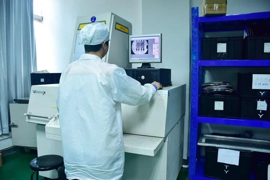
12. How does APTPCB handle BGA inspection? We utilize advanced 3D X-ray capabilities for NPI and complex assemblies. We combine this with SPI (Solder Paste Inspection) to prevent defects before the component is even placed.
Related pages & tools
- PCB Manufacturing Services: Explore our capabilities for high-layer count and HDI boards suitable for BGA assembly.
- X-ray inspection: Learn how we inspect hidden solder joints (voiding, HiP) during PCBA.
- Contact Us: Get technical support for your specific BGA reliability requirements.
- DFM Guidelines: Download our design rules to optimize your layout for manufacturing and inspection.
Glossary (key terms)
| Term | Definition |
|---|---|
| BGA (Ball Grid Array) | A surface-mount packaging used for integrated circuits where pins are replaced by a grid of solder balls. |
| Head-in-Pillow (HiP) | A defect where the BGA ball rests on the solder paste but fails to coalesce into a single joint. |
| Voiding | The presence of air or gas pockets trapped inside a solder joint. |
| Laminography | A 3D X-ray technique that creates cross-sectional slices of the PCB, allowing inspection of specific layers. |
| Intermetallic Compound (IMC) | The chemical layer formed between the solder and the copper pad; essential for a bond but brittle if too thick. |
| Coplanarity | The maximum distance between the highest and lowest solder ball on a component; poor coplanarity leads to open joints. |
| Wetting | The ability of molten solder to spread across and bond with a metal surface. |
| Reflow Profile | The temperature-vs-time curve a PCB undergoes in the oven; critical for activating flux and melting solder. |
| Stand-off Height | The distance between the bottom of the component body and the surface of the PCB after soldering. |
| IPC-7095 | The industry standard specifically guiding the design and assembly process implementation for BGAs. |
Conclusion
Mastering the x-ray criteria for bga voiding and head-in-pillow is not just about meeting a standard; it is about ensuring the longevity and safety of the final product. By adhering to IPC limits, utilizing 3D inspection techniques, and understanding the root causes of defects, engineers can virtually eliminate field failures related to BGA assembly.
At APTPCB, we integrate these rigorous inspection protocols into our standard workflow. From strict incoming quality control (iqc) checklist for pcba procedures to advanced X-ray analysis, we ensure every board meets the highest reliability standards. If you are dealing with complex BGA designs or reliability challenges, reach out to our engineering team for a comprehensive review.