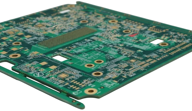
Intel Xeon processors serve as the backbone of modern data centers, driving everything from cloud computing to high-frequency trading. However, the processor is only as effective as the Xeon Server PCB that supports it. As data rates climb with PCIe Gen 5 and Gen 6 standards, the physical circuit board transforms from a simple carrier into a complex, active component of the signal channel.
Manufacturing these boards requires strict adherence to signal integrity, thermal management, and mechanical stability. At APTPCB (APTPCB PCB Factory), we see firsthand that successful server deployment depends on bridging the gap between high-level design simulation and the realities of mass production. This guide covers the entire lifecycle of a server board, ensuring your infrastructure meets the rigorous demands of modern computing.
Key Takeaways
- Signal Integrity is Paramount: Xeon platforms utilizing PCIe Gen 5 require ultra-low loss materials (like Megtron 6 or equivalent) to minimize signal attenuation.
- Layer Count Complexity: Most Xeon designs range from 12 to 24 layers, requiring precise registration and lamination cycles to prevent skew.
- Backdrilling is Mandatory: To reduce signal reflection in high-speed links, via stubs must be removed through controlled depth drilling (backdrilling).
- Thermal Management: High TDP (Thermal Design Power) processors demand heavy copper layers and careful thermal via placement to dissipate heat effectively.
- Validation Standards: Standard electrical testing is insufficient; Time Domain Reflectometry (TDR) and Interconnect Stress Testing (IST) are critical for reliability.
- Manufacturing Partner: Working with an experienced fabricator like APTPCB ensures that DFM (Design for Manufacturing) issues are caught before production begins.
What Xeon Server PCB really means (scope & boundaries)
Before diving into specific metrics, we must define the scope and physical boundaries that distinguish a Xeon Server PCB from standard consumer electronics.
A Xeon Server PCB is a high-performance printed circuit board specifically engineered to support Intel Xeon Scalable processors (and their supporting chipsets). Unlike a standard desktop motherboard, these boards are designed for 24/7 continuous operation, massive I/O throughput, and significant power delivery requirements.
The scope of these boards includes:
- Socket Support: Complex BGA or LGA footprints (e.g., LGA 4189, LGA 4677) with thousands of pins requiring high-density interconnects (HDI).
- High-Speed Channels: Routing for DDR5 memory and PCIe lanes where trace geometry must be controlled within microns to maintain impedance.
- Power Integrity: A Power Delivery Network (PDN) capable of supplying hundreds of amps at low voltages with minimal ripple.
The boundary of this technology lies in the materials and fabrication techniques. You cannot use standard FR4 for the high-speed layers of a modern Xeon board. The dielectric loss would destroy the signal integrity. Therefore, these PCBs are almost always hybrid builds, combining standard materials for power layers with advanced low-loss laminates for signal layers.
Xeon Server PCB metrics that matter (how to evaluate quality)
Once you understand the definition, you need quantifiable standards to measure the quality and performance of the board.
The following metrics are non-negotiable for server-grade hardware. If a manufacturer cannot provide data or guarantees on these figures, the board is at risk of failure in the field.
| Metric | Why it matters | Typical Range / Factor | How to measure |
|---|---|---|---|
| Differential Impedance | Ensures signal integrity for PCIe and DDR lines. Mismatches cause reflections and data loss. | 85Ω or 100Ω ±5% (stricter than standard ±10%). | Time Domain Reflectometry (TDR) coupons. |
| Dielectric Constant (Dk) | Determines signal propagation speed. Lower Dk is better for high speed. | 3.0 – 3.7 (Low-loss materials). | Resonator method or material datasheet verification. |
| Dissipation Factor (Df) | Measures how much signal energy is lost as heat in the material. | < 0.005 (Ultra-low loss). | Vector Network Analyzer (VNA). |
| Glass Transition Temp (Tg) | The temperature where the PCB becomes mechanically unstable. | > 170°C (High Tg is mandatory for lead-free assembly). | TMA (Thermomechanical Analysis). |
| Decomposition Temp (Td) | The temperature where the material loses 5% of its weight. | > 340°C. | TGA (Thermogravimetric Analysis). |
| Bow and Twist | Flatness is critical for large BGA/LGA socket soldering. | < 0.75% (Standard), < 0.5% (Server grade). | Laser profilometry or feeler gauges on a surface plate. |
| Conductive Anodic Filament (CAF) Resistance | Prevents internal shorts between vias over time due to electrochemical migration. | Must pass 1000 hours at 85°C/85% RH. | High-voltage bias testing in environmental chambers. |
How to choose Xeon Server PCB: selection guidance by scenario (trade-offs)
Metrics provide the data, but your specific deployment scenario dictates which metrics take priority and how you balance cost versus performance.
Different server form factors and applications impose unique constraints. Here is how to choose the right PCB specification based on your architecture.
1. 1U Server PCB vs. 4U Server PCB
- 1U Server PCB:
- Constraint: Vertical height is severely limited. Airflow is high-velocity but restricted volume.
- PCB Impact: Components must be low-profile. The PCB often requires high-thermal-conductivity materials because heat sinks are smaller.
- Trade-off: You may need to use Heavy Copper PCBs to handle power distribution without bulky busbars.
- 4U Server PCB:
- Constraint: Large physical size, heavy components (multiple GPUs, large heatsinks).
- PCB Impact: Mechanical rigidity is critical. The board thickness is often increased to 2.4mm or 3.0mm (standard is 1.6mm) to prevent sagging under the weight of the CPU coolers.
- Trade-off: Thicker boards make aspect ratios for plating vias more difficult, potentially increasing manufacturing cost.
2. AI Server PCB vs. Standard Web Server
- AI Server PCB:
- Requirement: Massive bandwidth between CPUs and GPUs (NVLink or similar).
- PCB Impact: Requires the highest grade of Ultra-Low Loss materials (e.g., Megtron 7 or Tachyon). Layer counts often exceed 20 to accommodate dense routing.
- Trade-off: Extremely high material cost and longer lead times.
- Standard Web Server:
- Requirement: Cost-efficiency and reliability for moderate workloads.
- PCB Impact: Can often use Mid-Loss materials or hybrid stackups (Low loss for signals, FR4 for power) to save money.
- Trade-off: Limited upgrade path for future high-speed interfaces.
3. Xeon Server PCB vs. ARM Server PCB
- Xeon Architecture:
- Focus: High single-thread performance and complex instruction sets.
- PCB Impact: Power delivery is complex due to turbo boost states causing rapid current spikes. The PDN impedance must be extremely low.
- ARM Architecture:
- Focus: Efficiency and parallel throughput.
- PCB Impact: Often requires more physical space for a higher number of smaller cores and memory channels spread out, leading to larger board footprints but potentially simpler thermal management per square inch.
4. High-Frequency Trading (HFT)
- Priority: Latency is the only metric that matters.
- PCB Choice: Use PTFE-based materials (Teflon) usually reserved for RF applications. Trace lengths must be length-matched to incredibly tight tolerances (mil-spec).
- Trade-off: These materials are difficult to process (drilling and plating) and expensive.
5. Edge Computing / Industrial Servers
- Priority: Durability in harsh environments.
- PCB Choice: Requires high-reliability surface finishes like ENEPIG. Conformal coating is often applied post-assembly.
- Trade-off: Testing requirements are higher (vibration, thermal shock) compared to climate-controlled data centers.
6. Storage Server (Cold Storage)
- Priority: Connectivity for many drives (SATA/SAS).
- PCB Choice: Often utilizes a Backplane PCB architecture. The main controller board connects to a large passive backplane.
- Trade-off: Signal integrity over long backplane traces requires careful simulation and potentially the use of repeaters/retimers.
Xeon Server PCB implementation checkpoints (design to manufacturing)

Selecting the right strategy is only the first step; execution requires a rigorous checkpoint process to ensure the design is manufacturable.
At APTPCB, we recommend the following 10-step checklist to guide your project from design file to finished board.
1. Stackup Design & Impedance Modeling
- Recommendation: Define the layer stackup before routing. Consult with the fabricator to use stocked materials.
- Risk: Designing a stackup that requires custom-order prepreg thicknesses can add weeks to lead time.
- Acceptance: Approved stackup diagram with calculated impedance values for all signal layers.
2. Material Selection & Hybrid Builds
- Recommendation: Use hybrid stacks (High-speed material for signals, FR4 for power/ground) to balance cost.
- Risk: CTE (Coefficient of Thermal Expansion) mismatch between different materials can cause delamination during reflow.
- Acceptance: Review material datasheets for CTE compatibility (Z-axis expansion).
3. Via Design & Aspect Ratio
- Recommendation: Keep via aspect ratios (Board Thickness : Drill Diameter) below 10:1 for standard production, or 12:1 for advanced.
- Risk: High aspect ratios lead to poor plating in the center of the via barrel, causing open circuits.
- Acceptance: DFM review report confirming all vias meet aspect ratio capabilities.
4. Backdrilling Definition
- Recommendation: Clearly identify nets requiring backdrilling in the design files.
- Risk: Missing backdrills on high-speed lines (PCIe Gen 5) creates stubs that act as antennas, ruining signal integrity.
- Acceptance: Verify the "Must Not Cut" layers and backdrill depth tolerance (typically ±0.15mm).
5. Thermal Management Strategy
- Recommendation: Use thermal vias under the CPU and VRMs. Consider coin-embed or heavy copper if heat is extreme.
- Risk: Insufficient copper weight leads to voltage droop and overheating.
- Acceptance: Thermal simulation results matching the copper weight specified in the fabrication notes.
6. Anti-Pad & Plane Clearance
- Recommendation: Increase anti-pad size on high-speed vias to reduce parasitic capacitance.
- Risk: Small clearances can cause shorts during registration misalignment or increase capacitance too much.
- Acceptance: Signal Integrity simulation (SI) confirming return loss is acceptable.
7. Surface Finish Selection
- Recommendation: Use ENIG (Electroless Nickel Immersion Gold) or OSP for flat pads on fine-pitch BGAs.
- Risk: HASL (Hot Air Solder Leveling) is too uneven for large LGA/BGA sockets.
- Acceptance: Specification of ENIG with proper gold thickness (2-5µin).
8. Panelization & Tooling Strips
- Recommendation: Ensure the panel has sufficient tooling strips and fiducials for automated assembly.
- Risk: Large server boards are heavy; weak panel tabs can break during handling.
- Acceptance: Panel drawing approval showing breakout tabs or V-score locations.
9. Electrical Testing Protocols
- Recommendation: Specify IPC Class 3 testing requirements.
- Risk: Standard "continuity only" testing might miss high-resistance latent defects.
- Acceptance: 100% Netlist testing certificate.
10. Final Quality Audit (FQA)
- Recommendation: Visual inspection for bow/twist and solder mask registration.
- Risk: Warped boards will fail to solder correctly during the SMT reflow process.
- Acceptance: QC report confirming bow/twist is within 0.5%.
Xeon Server PCB common mistakes (and the correct approach)
Even with a solid implementation plan, specific manufacturing pitfalls can derail a Xeon project. Here are the most common errors we see and how to avoid them.
1. Ignoring Resin Starvation in High-Copper Designs
- The Mistake: Using standard prepreg between heavy copper layers (2oz+). The resin flows into the gaps between copper features, leaving "dry" spots that delaminate.
- The Fix: Use High-Flow or High-Resin-Content prepreg (e.g., 1080 or 2116 glass styles) to ensure complete void filling.
2. Neglecting Fiber Weave Effect
- The Mistake: Routing high-speed differential pairs parallel to the glass weave of the PCB material. This causes periodic impedance variations (skew) as one trace runs over glass and the other over resin.
- The Fix: Route traces at a slight angle (zigzag routing) or use "Spread Glass" materials where the weave is tighter and more uniform.
3. Overlooking Via-in-Pad Plating Quality
- The Mistake: Placing vias in BGA pads without proper filling and capping (VIPPO). Solder wicks down the via during assembly, starving the joint.
- The Fix: Specify IPC-4761 Type VII (Filled and Capped) for all vias located within component pads.
4. Incorrect Backdrill Depth Tolerance
- The Mistake: Specifying a backdrill depth that is too close to the target signal layer. Manufacturing tolerances might cause the drill to cut the active trace.
- The Fix: Leave a safety margin (stub) of at least 8-10 mils (0.2mm - 0.25mm). While a shorter stub is better for signals, cutting the connection is catastrophic.
5. Poor Reference Plane Management
- The Mistake: Routing signals over a split in the ground plane. This increases loop inductance and causes EMI (Electromagnetic Interference) failures.
- The Fix: Ensure continuous ground reference planes for all high-speed signals. Use stitching capacitors if layer transitions are unavoidable.
6. Underestimating Lead Times for Advanced Materials
- The Mistake: Assuming Megtron PCB materials are in stock like FR4.
- The Fix: These materials often have 4-6 week lead times. Order materials as soon as the stackup is finalized, even before the layout is complete.
Xeon Server PCB FAQ (cost, lead time, materials, testing, acceptance criteria)
To address lingering uncertainties after reviewing common mistakes, here are answers to specific production questions regarding Xeon Server PCBs.
Q: What is the primary cost driver for a Xeon Server PCB? A: The primary drivers are layer count and material type. A 20-layer board using Megtron 6 will cost significantly more than a 10-layer FR4 board. Secondary drivers include the number of backdrilled holes and the density of HDI (High Density Interconnect) features like blind/buried vias.
Q: How does lead time differ for Server PCBs compared to standard PCBs? A: Standard PCBs can be turned around in 24-48 hours. Xeon Server PCBs typically require 10-15 working days due to complex lamination cycles (sequential lamination), backdrilling processes, and rigorous impedance testing. Material procurement can add additional time.
Q: Can I use FR4 for a PCIe Gen 5 Xeon board? A: No. Standard FR4 has a Dissipation Factor (Df) that is too high (~0.02), causing excessive signal loss at the frequencies required for PCIe Gen 5 (32 GT/s). You must use Low-Loss or Ultra-Low-Loss materials (Df < 0.005).
Q: What are the acceptance criteria for impedance control on these boards? A: For server applications, the standard tolerance is ±10%, but high-speed lines often require ±5%. This requires the manufacturer to perform TDR testing on test coupons included on the production panel. If the coupon fails, the board is rejected.
Q: Why is "Low Profile Copper" recommended for Server PCBs? A: At high frequencies, the "Skin Effect" forces current to flow along the outer surface of the conductor. Rough copper surfaces increase resistance and signal loss. Low Profile (LP) or Very Low Profile (VLP) copper foil is smoother, reducing insertion loss.
Q: Do I need to test every single board? A: Yes. For Server and Data Center PCBs, 100% electrical testing (Flying Probe or Bed of Nails) is mandatory to check for opens and shorts. Additionally, a sample percentage should undergo reliability testing like thermal shock or microsection analysis.
Q: How do I validate the reliability of the vias in a high-layer count board? A: Interconnect Stress Testing (IST) is the industry standard. It cycles the temperature of the vias to check for barrel cracks or post separation. This is more effective than standard thermal cycling for detecting via reliability issues.
Q: What is the risk of "Pad Cratering" in Xeon assemblies? A: Pad cratering occurs when the resin under a BGA pad fractures due to mechanical stress. This is common in stiff, high-Tg server boards. Using materials with a high fracture toughness and optimizing the cooling profile during assembly helps mitigate this.
Resources for Xeon Server PCB (related pages and tools)
To further assist in your engineering and procurement process, we have curated a list of internal resources and tools specifically relevant to server board design.
- Material Data: Deep dive into High Speed PCB materials and their properties.
- Stackup Planning: Understand how to build a Multilayer PCB structure that balances signal integrity and manufacturability.
- Design Guidelines: Review our DFM Guidelines to ensure your layout is ready for production.
- Impedance Tools: Use our Impedance Calculator for initial stackup estimation.
Xeon Server PCB glossary (key terms)
Finally, to ensure clear communication during the FAQ and quoting process, refer to these standard definitions used by engineers and fabricators.
| Term | Definition |
|---|---|
| Backdrilling | The process of drilling out the unused portion of a plated through-hole (stub) to reduce signal reflection. |
| BGA (Ball Grid Array) | A type of surface-mount packaging used for Xeon processors where connections are made via a grid of solder balls. |
| Blind Via | A via that connects an outer layer to one or more inner layers but does not go through the entire board. |
| Buried Via | A via connecting inner layers only; it is not visible from the outside of the board. |
| CTE (Coeff. of Thermal Expansion) | A measure of how much a material expands when heated. Mismatch in CTE causes reliability issues. |
| Differential Pair | Two complementary signals used to transmit data (e.g., PCIe, USB) with high noise immunity. |
| Dk (Dielectric Constant) | The ratio of the permittivity of a substance to the permittivity of free space. Affects signal speed. |
| Df (Dissipation Factor) | A measure of the power loss rate of an electrical oscillation in a dissipative system (signal loss). |
| HDI (High Density Interconnect) | PCB technology using microvias, fine lines, and spaces to achieve high circuit density. |
| Insertion Loss | The loss of signal power resulting from the insertion of a device (or trace) in a transmission line. |
| LGA (Land Grid Array) | A socket style where the pins are on the socket, and the processor has flat contact pads. |
| Skew | The time difference between the arrival of signals that should arrive simultaneously (e.g., within a diff pair). |
| Stackup | The arrangement of copper layers and insulating layers (prepreg/core) in a PCB. |
| Tg (Glass Transition Temp) | The temperature region where the base material changes from a glassy, solid state to a rubbery state. |
| TDR (Time Domain Reflectometry) | A measurement technique used to determine the characteristic impedance of PCB traces. |
Conclusion (next steps)
Designing and manufacturing a Xeon Server PCB is a discipline that tolerates no shortcuts. From the initial selection of low-loss materials to the final impedance validation, every step impacts the performance of the data center. As server architectures evolve toward AI-driven workloads and higher PCIe standards, the partnership between the design team and the manufacturer becomes the critical link in the supply chain.
At APTPCB, we specialize in the complexities of high-layer, high-speed server boards. Whether you are prototyping a new AI accelerator or scaling production for a 1U rackmount unit, our engineering team is ready to review your data.
Ready to move forward? To get an accurate DFM review and quote for your Xeon Server PCB, please prepare the following:
- Gerber Files (RS-274X): Including all copper, drill, solder mask, and silk layers.
- Fabrication Drawing: Specifying material requirements (e.g., "Panasonic Megtron 6 or equivalent"), stackup details, and impedance tables.
- Drill Chart: Clearly indicating backdrill locations and depths.
- Netlist: For IPC Class 3 electrical testing validation.
- Volume & Lead Time: Estimated annual usage and prototype urgency.
Contact us today to ensure your server infrastructure is built on a foundation of quality and reliability.