Z-Wave Light PCB quick answer (30 seconds)
Designing a Z-Wave Light PCB requires balancing high-voltage lighting control with sensitive Sub-GHz RF communication. Unlike 2.4 GHz protocols (Bluetooth, Zigbee), Z-Wave operates at 800–900 MHz, offering better wall penetration but requiring larger antennas and specific layout care.
- Frequency Specificity: You must design the antenna matching network for the specific region (e.g., 908.4 MHz for US, 868.4 MHz for Europe).
- Isolation is Critical: Lighting PCBs often handle AC mains. You must maintain strict creepage and clearance between the High Voltage (HV) AC side and the Low Voltage (LV) Z-Wave logic side.
- Antenna Clearance: Metal casings and LED heat sinks detune antennas. Maintain a minimum 10–15mm clearance around the antenna trace or chip antenna.
- Thermal Management: LED drivers generate heat. Use thermal vias or Metal Core PCBs (MCPCB) to prevent heat from drifting the frequency of the Z-Wave crystal oscillator.
- Module vs. SoC: For faster time-to-market, use pre-certified Z-Wave modules (e.g., Silicon Labs 700/800 series) rather than a chip-down design.
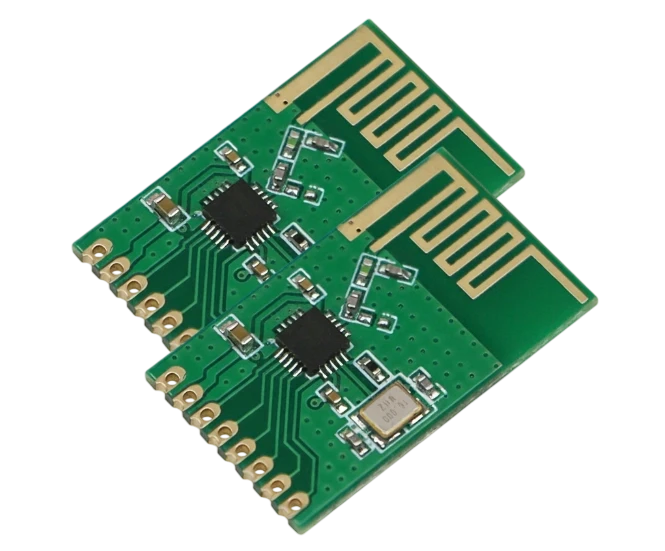
- Impedance Control: RF traces connecting the Z-Wave SoC to the antenna must be impedance matched (usually 50Ω) to prevent signal reflection and range loss.
When Z-Wave Light PCB applies (and when it doesn’t)
Z-Wave is a dominant standard in home automation, particularly for lighting, due to its mesh networking capabilities and lack of interference with Wi-Fi. However, it is not the universal solution for every smart light application.
Use Z-Wave Light PCB when:
- Whole-home automation is required: The device needs to act as a repeater node to strengthen the mesh network for other devices like locks or sensors.
- Long-range indoor penetration is needed: You need the signal to pass through thick concrete or brick walls where 2.4 GHz (Wi-Fi/Bluetooth) fails.
- Interoperability is a priority: The product must work seamlessly with established ecosystems like Samsung SmartThings, Hubitat, or Ring Alarm.
- Low power latency is critical: You need instant response times (FLiRS technology) for battery-operated switches or sensors without draining power.
- Security is paramount: The application requires S2 Security framework compliance, which is mandatory for Z-Wave certification.
Do not use Z-Wave Light PCB when:
- High data bandwidth is needed: Z-Wave data rates (up to 100 kbps) are insufficient for streaming audio or video; use Wi-Fi for those features.
- Global SKU simplicity is required: Z-Wave uses different frequencies in different countries, requiring multiple PCB variants (unlike 2.4 GHz Bluetooth/Thread which works globally).
- Ultra-low cost is the only driver: The cost of Z-Wave silicon and the mandatory certification process is generally higher than generic proprietary RF solutions.
- Direct phone control is needed without a hub: Z-Wave devices typically require a gateway/hub; they cannot connect directly to a smartphone like a Bluetooth Light PCB.
Z-Wave Light PCB rules and specifications (key parameters and limits)
Successful integration of Z-Wave into lighting products depends on strict adherence to RF and electrical safety rules. Below are the critical specifications for engineering a robust board.
| Rule / Parameter | Recommended Value / Range | Why it matters | How to verify | If ignored |
|---|---|---|---|---|
| RF Trace Impedance | 50Ω ±10% | Ensures maximum power transfer from the radio to the antenna. | TDR (Time Domain Reflectometry) testing on coupons. | Signal reflection causes poor range and high packet loss. |
| Antenna Keep-out | >10mm (3D space) | Nearby copper, metal, or components detune the antenna and absorb RF energy. | Review Gerber layers and 3D mechanical CAD. | Drastically reduced range; device becomes "deaf." |
| Crystal Tolerance | ±10 ppm | Z-Wave requires precise timing for frequency hopping and mesh synchronization. | Check component datasheet and load capacitance. | Device fails to join network or drops connection frequently. |
| HV/LV Isolation | >6.4mm (Reinforced) | Prevents 110/220V mains from arcing to the low-voltage user interface or antenna. | Hi-Pot testing (Dielectric Withstand) at 3000V+. | Safety hazard; electric shock risk; certification failure. |
| PCB Material (RF) | FR-4 (Tg >150°C) | Standard FR-4 is usually sufficient for Sub-GHz, but consistency is key. | Verify Dielectric Constant (Dk) stability with fab house. | Impedance mismatch if Dk varies significantly between batches. |
| Thermal Vias | 0.3mm hole, 0.6mm pitch | Dissipates heat from the dimmer TRIAC or LED driver away from the Z-Wave SoC. | Thermal simulation or IR camera testing on prototype. | Oscillator drift due to heat; shortened component lifespan. |
| Ground Plane | Solid, unbroken under RF | Provides a return path for RF signals and shields against noise. | Visual inspection of inner layers; check for "islands." | High EMI emissions; poor receiver sensitivity. |
| Decoupling Caps | Place <2mm from pin | Filters high-frequency noise from the power supply line entering the SoC. | Review placement in layout software. | Unstable operation; random resets; radio noise. |
| Copper Weight | 1 oz or 2 oz | Lighting circuits often carry high current; thicker copper manages heat and current. | Specify in fabrication notes. | Traces overheat or burn out under full lighting load. |
| Z-Wave Region | 868 MHz / 908 MHz / 921 MHz | Hardware matching network must align with the target market's frequency. | Network Analyzer (VNA) sweep of the antenna port. | Product works in the lab but fails in the target country. |
Z-Wave Light PCB implementation steps (process checkpoints)

APTPCB (APTPCB PCB Factory) recommends following a structured design process to minimize RF iterations.
Regional Frequency Selection:
- Action: Determine the target market (e.g., US, EU, ANZ) immediately.
- Key Parameter: SAW filter and antenna matching network values change based on frequency.
- Check: Confirm the BOM matches the regional frequency requirement.
SoC vs. Module Decision:
- Action: Choose between a SiP (System in Package) module or a discrete SoC design.
- Key Parameter: PCB area vs. Certification cost. Modules save certification time.
- Check: Verify if the module footprint fits within the lighting housing (e.g., bulb base or gang box).
Schematic Design & Power Supply:
- Action: Design a clean AC-DC power supply (SMPS) to step down mains voltage to 3.3V.
- Key Parameter: Ripple voltage <50mV.
- Check: Ensure the switching frequency of the power supply does not create harmonics in the 800–900 MHz band.
Stackup & Impedance Definition:
- Action: Define the layer stackup with the PCB manufacturer.
- Key Parameter: Dielectric thickness between Top Layer (RF) and Layer 2 (Ground).
- Check: High Frequency PCB guidelines for controlled impedance.
Layout & Antenna Placement:
- Action: Place the antenna first, at the edge of the board, away from the AC power entry.
- Key Parameter: Keep-out zone dimensions.
- Check: Run a DRC (Design Rule Check) specifically for antenna clearance.
Thermal Management Layout:
- Action: Route high-current tracks for the lighting load and place thermal vias under MOSFETs/TRIACs.
- Key Parameter: Junction temperature (Tj) max.
- Check: Ensure heat does not flow directly toward the Z-Wave crystal.
DFM Review:
- Action: Submit Gerbers for Design for Manufacturing review.
- Key Parameter: Minimum trace width/spacing and drill sizes.
- Check: DFM Guidelines to prevent manufacturing defects.
Prototyping & Assembly:
- Action: Manufacture the bare board and assemble components (SMT).
- Key Parameter: Solder paste profile (reflow temperature).
- Check: Inspect solder joints on the fine-pitch Z-Wave module/SoC.
RF Tuning & Validation:
- Action: Use a VNA to measure the antenna return loss (S11).
- Key Parameter: S11 < -10dB at center frequency.
- Check: Adjust the Pi-network (inductors/capacitors) to center the resonance.
Z-Wave Certification Pre-scan:
- Action: Test for compliance with Z-Wave Alliance standards.
- Key Parameter: RF power output and receiver sensitivity.
- Check: Verify the device includes/excludes from a standard Z-Wave controller.
Z-Wave Light PCB troubleshooting (failure modes and fixes)
Even with good design, issues arise during testing. Use this logic flow to diagnose common Z-Wave lighting faults.
Symptom: Device pairs but has very short range (<5 meters).
- Cause: Antenna detuning due to housing or mismatch.
- Check: Is the PCB installed in a metal box? Is the matching network tuned for the bare board or the final assembly?
- Fix: Retune the antenna matching network with the plastic housing and final mechanics in place.
- Prevention: Simulate the housing material (dielectric) during the design phase.
Symptom: Light flickers or strobes when Z-Wave radio transmits.
- Cause: Power supply noise or voltage sag. The RF transmission (TX) current spike drops the 3.3V rail, affecting the LED driver control signal.
- Check: Monitor the 3.3V rail with an oscilloscope during TX bursts.
- Fix: Increase bulk capacitance on the 3.3V rail; add ferrite beads between the RF section and the LED driver section.
- Prevention: Separate the power domains for the radio and the lighting control logic.
Symptom: Device drops off the network after a few hours.
- Cause: Crystal oscillator frequency drift due to heat.
- Check: Measure the temperature near the crystal after the light has been on at 100% brightness for 1 hour.
- Fix: Improve thermal isolation; move the crystal further from the heat source; use a high-temperature rated crystal.
- Prevention: Use Metal Core PCB technology for better heat dissipation if using high-power LEDs.
Symptom: Cannot include (pair) the device.
- Cause: Region mismatch or lack of DSK (Device Specific Key) entry for S2 security.
- Check: Verify the Z-Wave module frequency matches the controller. Check if the controller requires the QR code scan (SmartStart).
- Fix: Reset the device to factory default; ensure the correct region firmware is loaded.
- Prevention: Clearly label PCBs with region codes during production.
Symptom: High EMI failures during certification.
- Cause: Harmonics from the LED driver switching frequency coupling onto the antenna.
- Check: Run a near-field probe scan over the board.
- Fix: Add shielding cans over the LED driver circuitry; improve grounding stitching.
- Prevention: Keep the antenna trace as far as possible from the switching node of the power supply.
How to choose Z-Wave Light PCB (design decisions and trade-offs)
When developing a smart lighting product, engineers often compare Z-Wave Light PCB against other protocols like Bluetooth Light PCB, Matter Light PCB, or Thread Light PCB.
1. Range and Penetration
- Z-Wave: Operates at ~900 MHz. Wavelength is longer, allowing it to pass through walls, furniture, and floors better than 2.4 GHz signals. Ideal for large homes or concrete structures.
- Bluetooth/Thread/Matter (over Thread): Operate at 2.4 GHz. Signals are more easily absorbed by water (people) and obstacles. Requires more repeater nodes to cover the same area.
2. Network Topology
- Z-Wave: Uses a source-routed mesh. The controller knows the path. It is highly stable for static devices like light switches. Limit of 232 nodes (historically), though Z-Wave Long Range extends this.
- Bluetooth Mesh: Uses managed flooding. robust but can be "noisy" on the spectrum.
- Thread/Matter: IP-based mesh. Self-healing and very robust, but the ecosystem is still maturing compared to the established Z-Wave market.
3. Power Consumption (for Sensors/Switches)
- Z-Wave: Excellent for battery-operated sensors or switches linked to lights (using FLiRS).
- Wi-Fi: Too power-hungry for battery-operated lighting controls.
- Bluetooth LE: Very low power, but range is the limitation.
4. Cost and Ecosystem
- Z-Wave: Chips are primarily from Silicon Labs (proprietary source), and certification is mandatory. This ensures high quality and interoperability but raises the BOM and NRE cost.
- Matter/Thread: Open standards with multiple silicon vendors (Nordic, TI, Silicon Labs, NXP). Competition may lower chip costs, but software complexity is higher.
Decision Matrix:
- Choose Z-Wave if you are building a premium home automation product where reliability, range, and security (S2) are non-negotiable.
- Choose Matter/Thread if you want future-proofing and IP-based connectivity.
- Choose Bluetooth if you want a simple, direct-to-phone connection without a hub.
Z-Wave Light PCB FAQ (cost, lead time, common defects, acceptance criteria, Design for Manufacturability (DFM) files)
What impacts the cost of a Z-Wave Light PCB? The primary cost drivers are the Z-Wave SoC/Module (single-source vendor), the PCB material (consistent FR-4 is required), and the layer count (usually 4 layers for impedance control). Additionally, the mandatory Z-Wave Alliance certification adds a fixed NRE cost to the project, unlike open 2.4 GHz standards.
What is the standard lead time for Z-Wave Light PCB prototypes? For standard FR-4 designs, APTPCB can deliver bare boards in 24–48 hours. However, if you require turnkey assembly including the Z-Wave module, lead time depends on component availability. Z-Wave silicon can sometimes have longer lead times than passive components; typically, turnkey prototypes take 1–2 weeks.
Which materials are best for Z-Wave Light PCB RF performance? Standard FR-4 with a high Tg (Glass Transition Temperature) of 150°C or 170°C is usually sufficient for Sub-GHz frequencies. Expensive PTFE or Rogers materials are rarely needed for Z-Wave unless the environment is extreme. The critical factor is the consistency of the Dielectric Constant (Dk) from the laminate supplier.
What testing is required for Z-Wave Light PCB acceptance? Acceptance criteria should include:
- Impedance Testing: Verification of 50Ω traces on coupons.
- Functional Test (FCT): Power up, pairing with a reference controller, and toggling the load.
- RF Power Measurement: Verifying TX power meets the region's limit (e.g., +13dBm).
- Hi-Pot Test: Ensuring isolation between AC mains and the logic/antenna section.
How do I prepare DFM files for a Z-Wave lighting project? When submitting to APTPCB, include:
- Gerber Files: RS-274X format.
- Stackup Drawing: Clearly specifying the dielectric thickness for impedance control.
- Drill File: Distinguishing between plated and non-plated holes (especially for antenna mounting).
- Assembly Drawing: Indicating the orientation of the Z-Wave module and antenna.
- BOM: Specifying the exact part number for the Z-Wave SoC/Module.
Can I use a chip antenna or a PCB trace antenna? Yes, both are common. A PCB trace antenna (like an inverted-F) is free (zero BOM cost) but requires more board space and careful tuning. A chip antenna saves space but adds cost ($0.20–$0.50) and introduces insertion loss. For light bulbs with tight space, a wire antenna or a custom stamped metal antenna is often used.
What are common defects in Z-Wave Light PCB manufacturing?
- Solder Voiding: Under the large ground pad of the Z-Wave module (QFN style), leading to poor grounding and thermal performance.
- Tombstoning: Of small 0402 matching network components due to uneven heating.
- Flux Residue: Conductive flux residue near the antenna can detune the frequency.
Does APTPCB support Z-Wave Long Range (LR) designs? Yes. Z-Wave LR operates on the same frequency but uses different modulation (DSSS OQPSK). The PCB design rules are identical, but the output power requirements may be higher (+14 dBm or +20 dBm), requiring robust power supply design and thermal dissipation strategies.
How does "SmartStart" affect PCB production? SmartStart allows devices to be paired via QR code before they are powered on. This requires the PCB assembler to print and adhere a unique QR code (containing the DSK) to the PCB or product housing during the Box Build Assembly process. The DSK must match the firmware flashed into the chip.
What is the difference between Z-Wave 700 and 800 series for PCB design? The 800 series offers better range and battery life. Pin compatibility varies between packages. From a PCB standpoint, the 800 series often requires fewer external passives, simplifying the layout, but the thermal and RF layout principles remain the same.
Resources for Z-Wave Light PCB (related pages and tools)
- High Frequency PCB Manufacturing: Capabilities for RF and impedance-controlled boards.
- SMT & THT Assembly: Details on assembling fine-pitch wireless modules.
- DFM Guidelines: Essential checklist before submitting your design.
- Impedance Calculator: Tool to estimate trace width for 50Ω matching.
Z-Wave Light PCB glossary (key terms)
| Term | Definition |
|---|---|
| Sub-GHz | Radio frequencies below 1 GHz (e.g., 868/908 MHz). Offers better range and penetration than 2.4 GHz. |
| Mesh Network | A network topology where devices (nodes) relay messages for other devices, extending total range. |
| FLiRS | Frequently Listening Receiver Slave. A battery-saving mode allowing devices to wake up instantly (latency <1s). |
| S2 Security | Security 2 framework. Mandatory encryption standard for Z-Wave devices to prevent hacking. |
| SmartStart | A feature allowing devices to be provisioned into the network by scanning a QR code before powering up. |
| Inclusion/Exclusion | The process of adding (pairing) or removing (unpairing) a device from the Z-Wave network. |
| Gateway / Hub | The central controller that manages the Z-Wave network and bridges it to the internet. |
| OTA (Over-The-Air) | The ability to update the device firmware wirelessly after installation. |
| Repeater | A mains-powered Z-Wave device that receives and re-transmits signals to extend network coverage. |
| Z-Wave Long Range | A star topology mode allowing direct hub-to-device communication over 1+ miles, bypassing the mesh. |
| SoC (System on Chip) | An integrated circuit that combines the Z-Wave radio, microcontroller, and memory in one package. |
| Matching Network | A circuit of inductors and capacitors used to match the impedance of the radio to the antenna. |
Request a quote for Z-Wave Light PCB (Design for Manufacturability (DFM) review + pricing)
Ready to move your smart lighting project from concept to production? APTPCB provides comprehensive DFM reviews to ensure your RF design is manufacturable and cost-effective.
What to send for an accurate quote:
- Gerber Files: Including all copper, solder mask, and drill layers.
- Stackup Requirements: Specify impedance control for RF traces (e.g., 50Ω on Layer 1).
- BOM (Bill of Materials): Highlight the Z-Wave module/SoC and any critical RF passives.
- Volume: Prototype quantity vs. estimated mass production volume.
- Testing Requirements: Specify if you need firmware flashing or functional testing.
Get Your Z-Wave PCB Quote Now – Our engineers will review your files and provide a price and lead time estimate within 24 hours.
Conclusion (next steps)
Successfully deploying a Z-Wave Light PCB requires more than just connecting a radio chip; it demands a holistic approach to RF tuning, thermal management, and safety isolation. By adhering to strict impedance rules, managing heat from LED drivers, and designing for the specific regional frequency, you ensure your product delivers the reliability and range that Z-Wave is famous for. Whether you are building a retrofit switch or a smart bulb, following these guidelines will streamline your path to certification and market launch.