
Contents
- Highlights
- Scope and Decision Context
- Specifications to Define Upfront
- Key Risks (Root Causes & Prevention)
- Validation & Acceptance Criteria
- Supplier Qualification Checklist
- Glossary
- 6 Essential Rules for Sourcing 5G Sa PCB (Cheat Sheet)
- FAQ
- Request a Quote / DFM Review for 5G Sa PCB
- Conclusion
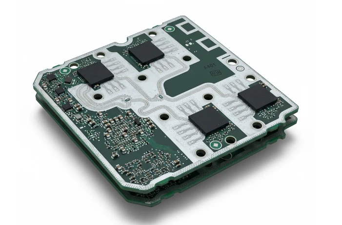
The shift from Non-Standalone (NSA) to Standalone (5G SA) networks represents a fundamental architectural change, not just a software upgrade. For the procurement engineer, this shift moves the goalposts significantly. If you source a 5G SA AAU (Active Antenna Unit) PCB using legacy 4G or even early 5G NSA specifications, you risk catastrophic signal loss, thermal runaway in Massive MIMO arrays, and unacceptable latency. In the 5G SA ecosystem, the PCB is no longer just a carrier; it is an active component of the RF signal path.
At APTPCB, we have seen buyers struggle with the "invisible" specs—surface roughness, passive intermodulation (PIM), and hybrid stack-up compatibility. Choosing the wrong laminate or neglecting the skin effect at sub-6GHz and mmWave frequencies can result in yield losses exceeding 40% during assembly. This playbook is designed to bridge the gap between RF engineering requirements and procurement execution, ensuring your 5G SA infrastructure is built on a foundation of reliability.
Highlights
- Material Selection is Critical: 5G SA demands ultra-low loss materials (Df < 0.003). Standard FR4 is insufficient for the RF path; hybrid stack-ups (FR4 + Rogers/Panasonic) are the standard for cost-efficiency.
- Thermal Management: Massive MIMO units generate immense heat. Metal-core PCBs, copper coins, and high-thermal conductivity prepregs are mandatory.
- Signal Integrity: Copper surface roughness (profile) directly impacts insertion loss. Specify HVLP (High VLP) or VLP copper.
- HDI & Layer Count: 5G SA BBU and AAU boards often require 12+ layers with Any-Layer HDI to manage high I/O density.
- PIM Control: Passive Intermodulation can degrade network throughput. Solder mask, surface finish, and etching quality must be controlled to minimize PIM.
- Backdrilling: Essential for reducing signal reflection (stub effect) in high-speed links (>10 Gbps).
Spec / Lever → Procurement Outcome
| Spec / Decision Lever | Outcome (Yield / Cost / Lead Time) |
|---|---|
| Hybrid Stack-up (FR4 + Rogers) | Reduces material cost by 30-40% vs. pure Rogers, but requires experienced lamination process to prevent delamination. |
| Copper Profile (HVLP) | Reduces insertion loss at high frequencies. Critical for 5G range and power efficiency. |
| Backdrilling (Stub Removal) | Improves Signal Integrity (BER). Adds 1-2 days to lead time but essential for >25Gbps data rates. |
| Immersion Silver / ENEPIG Finish | Lowers PIM and insertion loss compared to ENIG. Requires strict storage handling to prevent tarnishing. |
Scope and Decision Context
5G Standalone (SA) networks decouple the 5G Radio Access Network (RAN) from the 4G LTE core. This allows for the full realization of 5G benefits: ultra-low latency (uRLLC) and massive machine-type communications (mMTC). Consequently, the hardware requirements are stricter than NSA deployments.
This playbook applies specifically when you are sourcing PCBs for:
- AAU (Active Antenna Units): The radio head containing the antenna array and RF front end.
- BBU (Base Band Units): High-performance computing units processing baseband signals.
- Small Cells: Compact 5G nodes for indoor or dense urban coverage.
- RF Components: 5G ADC (Analog-to-Digital Converter) boards, Attenuators, and Baluns.
If you are sourcing for legacy LTE or sub-1GHz IoT devices, these specifications may be overkill. However, for any infrastructure operating in the C-Band (3.5GHz) or mmWave (24GHz+), the guidelines below are mandatory.
For a deeper dive into the manufacturing capabilities required for these frequencies, refer to our guide on High Frequency PCB Manufacturing.
Spec / Lever → Procurement Outcome
| Spec / Decision Lever | Outcome (Yield / Cost / Lead Time) |
|---|---|
| Dielectric Constant (Dk) Tolerance | Tight tolerance (±0.05) ensures consistent impedance. Loose tolerance leads to signal reflection and batch rejection. |
| Thermal Conductivity (>1.0 W/mK) | Prevents PA (Power Amplifier) overheating. Critical for AAU reliability in outdoor environments. |
| Aspect Ratio (Drill:Thickness) | High aspect ratios (>12:1) increase plating difficulty and cost. Keeping it <10:1 improves yield. |
| Solder Mask Color/Type | Specific low-loss solder masks are required. Standard green may have too high Df for mmWave traces. |
Specifications to Define Upfront
When issuing an RFQ for 5G SA PCBs, ambiguity is your enemy. "Standard IPC Class 2" is not enough. You must specify parameters that control signal integrity and thermal performance.
| Parameter | Standard Spec (Avoid for 5G SA) | High-Performance Spec (Required for 5G SA) | Why It Matters |
|---|---|---|---|
| Base Material | Standard FR4 (Tg 140) | High-Speed Low-Loss (Panasonic Megtron 6/7, Rogers RO4350B/RO3003, Isola Tachyon) | Standard FR4 absorbs too much signal at >3GHz. |
| Copper Foil | Standard ED Copper | HVLP (High Very Low Profile) or RTF | Rough copper acts like a resistor at high frequencies (Skin Effect). |
| Layer Count | 4-8 Layers | 12-30 Layers (often Hybrid) | High density required for Massive MIMO routing and power planes. |
| Impedance Control | ±10% | ±5% or ±7% | Mismatched impedance causes signal reflection and data loss. |
| Surface Finish | HASL / ENIG | Immersion Silver, ENEPIG, or OSP | ENIG's nickel layer is magnetic and causes insertion loss at high frequencies. |
| Via Technology | Through-hole | Blind/Buried Vias, Backdrilling, POFV | Reduces signal stubs and allows high-density BGA fanout. |
| Thermal Mgmt | Standard Vias | Copper Coin, Metal Core, Via-in-Pad | AAUs generate massive heat; standard dissipation is insufficient. |

The Hybrid Stack-up Strategy
To manage costs, most 5G SA AAUs use a Hybrid Stack-up. This involves using expensive high-frequency materials (like Rogers) only for the signal layers carrying RF traffic, and cheaper high-Tg FR4 for power, ground, and digital control layers.
- Buyer Note: Ensure your manufacturer has specific experience with hybrid lamination. The thermal expansion coefficients (CTE) of FR4 and Rogers materials differ, which can lead to warping or delamination during reflow if not managed correctly. See our Multilayer PCB capabilities for more on complex stack-ups.
Key Risks (Root Causes & Prevention)
Sourcing 5G SA PCBs introduces risks that are rare in consumer electronics. Understanding these root causes helps you ask the right questions during DFM (Design for Manufacturing).
1. Passive Intermodulation (Pim)
- The Issue: Two or more signals mix in a non-linear device (the PCB trace) to create interference frequencies that block the receiver.
- Root Cause: Rough copper, nickel in the surface finish (ENIG), contaminated etching, or poor solder mask adhesion.
- Prevention: Specify Immersion Silver or ENEPIG (if designed correctly). Ensure the fab uses "PIM-grade" copper foil.
2. Thermal Management Failure
- The Issue: The Power Amplifiers (PAs) in a Massive MIMO unit generate significant heat. If the PCB cannot dissipate this, the unit shuts down or degrades.
- Root Cause: Insufficient copper weight, lack of thermal vias, or using a dielectric with poor thermal conductivity.
- Prevention: Use embedded copper coins or heavy copper layers (3oz+). Validate the thermal via density in the DFM stage.
3. Signal Integrity Loss (Insertion Loss)
- The Issue: The signal weakens significantly as it travels across the board, reducing the range of the 5G tower.
- Root Cause: Using standard copper (too rough) or neglecting the "fiber weave effect" (where traces align with glass bundles in the laminate, causing impedance variance).
- Prevention: Specify HVLP copper. Request "spread glass" or "flat glass" styles (e.g., 1067, 1078) to mitigate the fiber weave effect.
4. Registration Errors in Hybrid Builds
- The Issue: Misalignment between the Rogers layers and FR4 layers.
- Root Cause: Different scaling factors (material movement) during the lamination heat cycle.
- Prevention: Choose a supplier with a proven track record in Rogers PCB Manufacturing. They will have calculated scaling factors for specific material combinations.
Validation & Acceptance Criteria
| Test / Check | Method | Pass criteria (example) | Evidence |
|---|---|---|---|
| Electrical continuity | Flying probe / fixture | 100% nets tested; no opens/shorts | E-test report |
| Critical dimensions | Measurement | Meets drawing tolerances | Inspection record |
| Plating / fill integrity | Microsection | No voids/cracks beyond IPC limits | Microsection photos |
| Solderability | Wetting test | Acceptable wetting; no de-wet | Solderability report |
| Warpage | Flatness measurement | Within spec (e.g., ≤0.75%) | Warpage record |
| Functional validation | FCT | All cases pass; log stored | FCT logs |
How do you ensure the PCBs you receive will perform in the field? You cannot rely solely on visual inspection. Implement this validation protocol.
Validation & Acceptance
Quality Assurance Standard Procedure
Time Domain Reflectometry (TDR) coupons must be tested on every panel. For 5G SA, ensure testing is done at relevant rise times. Verify tolerance is within ±5% or ±7% as specified.
For antenna boards, request Passive Intermodulation (PIM) testing on test coupons. This validates that the etching quality and surface finish are not generating interference.
Microsectioning is vital to verify layer alignment in hybrid stack-ups, hole wall plating thickness (min 20-25µm), and the effectiveness of backdrilling (stub length check).
Interconnect Stress Testing (IST) cycles the PCB through thermal extremes. This confirms that the different materials in a hybrid stack-up will not delaminate in the field.
Supplier Qualification Checklist
Before awarding a contract for 5G SA PCBs, use this checklist to audit potential suppliers. A "No" to any of these suggests they may not be ready for high-reliability 5G manufacturing.
- Hybrid Lamination Experience: Can the supplier provide case studies or evidence of successful FR4 + Rogers/Megtron hybrid builds?
- Backdrilling Capability: Do they have automated backdrilling equipment with depth control tolerance of ±0.05mm or better?
- Low-Roughness Copper Stock: Do they stock HVLP or VLP copper foils as standard for high-frequency orders?
- Impedance Modeling: Do they use advanced software (like Polar Si9000) to verify your stack-up before production?
- PIM Awareness: Does the QA team understand PIM (Passive Intermodulation) and how to test for it?
- Cleanliness Standards: Do they adhere to strict ionic contamination limits (critical for preventing electrochemical migration in outdoor AAUs)?
- Supply Chain Security: Do they have direct lines to authorized distributors for Rogers, Isola, and Panasonic materials to avoid counterfeits?
Glossary
5G SA (Standalone): A 5G network implementation that uses a 5G core network, independent of 4G LTE infrastructure. It enables advanced features like network slicing and ultra-low latency.
Massive MIMO: "Multiple-Input Multiple-Output." An antenna technology where the base station uses a large array of antennas (often 32 or 64) to transmit and receive data simultaneously, requiring complex, high-heat PCBs.
Dk (Dielectric Constant): A measure of a material's ability to store electrical energy. For 5G, a low and stable Dk is required to maintain signal speed and impedance control.
Df (Dissipation Factor): A measure of how much signal energy is lost as heat in the PCB material. 5G requires extremely low Df (<0.003) to preserve signal strength.
PIM (Passive Intermodulation): Signal interference generated by non-linearities in the passive components (like the PCB traces, connectors, or solder joints), often caused by poor manufacturing quality.
Backdrilling: The process of drilling out the unused portion of a plated through-hole (via stub) to reduce signal reflection in high-speed circuits.
6 Essential Rules for Sourcing 5G Sa PCB (Cheat Sheet)
| Sourcing Rule | Why It Matters (Risk/Cost) | Procurement Action |
|---|---|---|
| 1. Don't Guess Dk/Df | Wrong values ruin impedance; board becomes scrap. | Specify exact material datasheet (e.g., "Rogers RO4350B") or equivalent performance specs. |
| 2. Specify Copper Profile | Standard copper kills high-freq signals (Skin Effect). | Explicitly request "HVLP" or "VLP" copper foil in the RFQ notes. |
| 3. Use Hybrid Stack-ups | Pure high-freq boards are 3x the cost. | Work with engineering to mix FR4 (power/digital) with Rogers (RF) layers. |
| 4. Thermal Vias are Mandatory | AAUs will overheat and fail without them. | Ensure BOM/Gerbers include thermal via arrays under PA components. |
| 5. Watch the Surface Finish | ENIG causes signal loss at >3GHz. | Switch to Immersion Silver or ENEPIG for RF boards. |
| 6. Prototype Before Production | Simulation vs. Reality gap is high in RF. | Run a small NPI batch to validate signal integrity and thermal performance. |
FAQ
Q: What is the main difference between 5G SA and NSA PCB requirements?
A: While NSA often utilizes existing LTE infrastructure, 5G SA (Standalone) requires a completely new core and radio network. This typically demands higher layer counts, lower latency performance, and stricter thermal management in the AAU due to the increased processing load of the 5G core protocols directly at the edge.
Q: Why are Hybrid Stack-ups recommended for 5G PCBs?
A: High-frequency materials like Rogers or Taconic are significantly more expensive than standard FR4. A hybrid stack-up uses the expensive material only for the layers carrying critical RF signals, while using FR4 for the remaining layers (power, ground, control). This provides the necessary performance at a much lower total unit cost.
Q: Can we use ENIG surface finish for 5G SA boards?
A: It is generally not recommended for high-frequency RF layers. ENIG contains a nickel layer which is ferromagnetic; this can cause significant insertion loss and PIM (Passive Intermodulation) at 5G frequencies. Immersion Silver or ENEPIG are preferred alternatives.
Q: What is the lead time impact of Backdrilling?
A: Backdrilling is a secondary drilling process used to remove conductive stubs from vias. It typically adds 1-2 days to the standard production lead time but is essential for signal integrity in high-speed data links (typically >10 Gbps).
Q: How do I validate the thermal performance of the PCB?
A: During the design phase, thermal simulation is key. During manufacturing validation, you should request thermal stress testing (like IST) to ensure the vias and material interfaces can withstand the heat cycles. For the finished PCBA, thermal imaging during functional testing is common.
Q: What is the "Skin Effect" and why does it matter for procurement?
A: At high frequencies (like 5G), electricity flows only along the outer "skin" of the copper conductor. If the copper surface is rough, the signal has to travel a longer path, causing resistance and signal loss. Procurement must specify "Low Profile" (VLP/HVLP) copper to minimize this.
Request a Quote / DFM Review for 5G Sa PCB
Ready to move your 5G SA project from design to production? To get an accurate quote and a comprehensive DFM (Design for Manufacturing) review, please provide the following:
- Gerber Files: RS-274X or ODB++ format.
- Stack-up Diagram: Clearly indicating material types (e.g., Rogers 4350B + FR4 TG170) and layer order.
- Impedance Requirements: Specific trace widths and target impedance values (e.g., 50Ω SE, 100Ω Diff).
- Drill Chart: Identifying any backdrilling requirements.
- Surface Finish: Specified (e.g., Immersion Silver).
- Quantity & Lead Time: Prototype vs. Mass Production volumes.
Conclusion
Sourcing PCBs for 5G Standalone networks is a high-stakes exercise in balancing cost, thermal performance, and signal integrity. The transition from "standard" manufacturing to "RF-grade" manufacturing requires a shift in mindset—from viewing the PCB as a simple connector to viewing it as a complex component of the antenna system.
By defining your materials explicitly, understanding the risks of PIM and thermal failure, and validating your suppliers against the checklist provided, you can secure high-yield production for your 5G infrastructure.
At APTPCB, we specialize in high-frequency, hybrid, and HDI technologies required for the 5G era. Whether you are building AAUs, BBUs, or specialized RF components, our engineering team is ready to support your deployment.
Signed, The Engineering Team at APTPCB