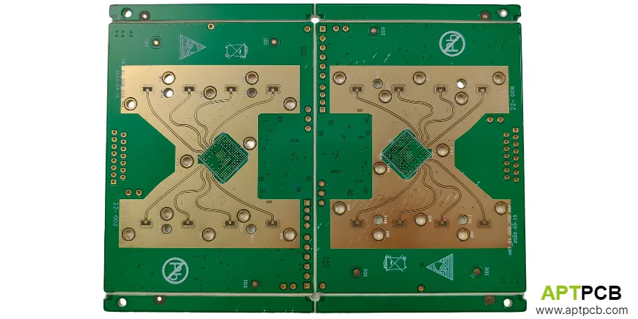
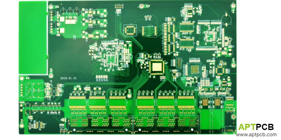
A high-frequency circuit board is a specialized printed circuit board engineered to maintain signal integrity at frequencies typically above 1 GHz, where standard FR-4 materials exhibit unacceptable loss, impedance variation, and dielectric instability. At these elevated frequencies, electromagnetic wave behavior dominates—traces function as transmission lines, parasitic elements become significant, and material properties directly determine circuit performance.
This guide explains the fundamental differences between standard and high-frequency circuit boards, helping engineers understand when specialized solutions become necessary and what factors determine high-frequency PCB performance.
Defining High-Frequency Circuit Board Operation
The distinction between standard and high-frequency operation emerges when signal wavelengths become comparable to physical circuit dimensions. This transition typically occurs above several hundred MHz for analog RF signals or when digital edge rates fall below 1 nanosecond regardless of clock frequency.
Consider wavelength: at 1 GHz, a signal has approximately 300mm wavelength in free space, reduced to roughly 150mm on a typical PCB substrate. At 10 GHz, wavelength shrinks to about 15mm on-board. When trace lengths approach these dimensions, the entire trace becomes an electromagnetic structure rather than a simple wire connecting two points.
Standard FR-4 circuit boards serve general electronics effectively, but their glass-reinforced epoxy construction exhibits fundamental limitations at elevated frequencies:
- Dielectric constant variation: FR-4 Dk varies ±10% across board area and changes with frequency and temperature, making precise impedance control impossible
- High dissipation factor: Df exceeds 0.02, causing approximately 0.5 dB/inch signal loss at 1 GHz—acceptable for short digital traces but problematic for RF paths
- Moisture sensitivity: Water absorption shifts dielectric properties, particularly problematic in humid environments
These characteristics, acceptable for power distribution and low-speed digital circuits, create unacceptable performance degradation in RF applications requiring consistent impedance and minimal loss.
Key High-Frequency Behavior Characteristics
- Transmission Line Effects: Signal traces exhibit characteristic impedance determined by geometry and materials. Mismatches cause reflections that degrade signal quality and power transfer efficiency—a 10% impedance mismatch reflects approximately 5% of signal power.
- Skin Effect Impact: Current concentrates near conductor surfaces at high frequencies, increasing effective resistance. At 1 GHz, skin depth in copper is approximately 2 micrometers, making surface roughness and finish quality critical.
- Dielectric Loss Significance: Substrate dissipation factor directly determines signal attenuation. Premium materials achieve 10x lower loss than standard FR-4, translating to several dB improvement over typical trace lengths.
- Parasitic Sensitivity: Via inductance (typically 0.5-1 nH), pad capacitance, and trace discontinuities create impedance variations negligible at low frequencies but significant at GHz operation.
- Wavelength Considerations: A 10 GHz signal has approximately 30mm wavelength in free space, shorter on PCB substrates. Circuit features become significant fractions of wavelength, requiring distributed circuit design approaches.
- Radiation Susceptibility: Improper trace routing or inadequate reference planes cause signal radiation and susceptibility to external interference.
Understanding these behaviors enables engineers to specify high-frequency circuit boards achieving required performance across intended operating ranges.
Understanding Critical Material Properties
Material selection fundamentally determines high-frequency circuit board performance. Two electrical properties dominate selection criteria: dielectric constant affecting impedance and signal velocity, and dissipation factor determining signal loss through the substrate.
Dielectric Constant (Dk)
Dielectric constant determines signal propagation velocity (approximately c/√Dk) and the trace dimensions required to achieve target impedance. More critically, Dk stability across frequency range, temperature excursions, and board area ensures predictable, consistent circuit behavior.
Standard FR-4 exhibits Dk variations of ±10% or more, rendering precise impedance control impossible. Premium high-frequency materials maintain Dk within ±2%, enabling reliable RF circuit implementation with impedance tolerances of ±5% achievable in production.
Dissipation Factor (Df)
Dissipation factor represents energy lost as signals propagate through the dielectric material. This loss accumulates along trace length following approximately:
Loss (dB/inch) ≈ 2.3 × f(GHz) × √Dk × Df
This relationship makes Df particularly critical for longer transmission lines and higher frequencies where loss per unit length increases. Premium PTFE-based materials achieve Df below 0.002 compared to FR-4's 0.02—a 10x improvement translating directly to preserved signal strength.
Key Material System Options
- PTFE Composites: Rogers RT/duroid series providing lowest loss tangent values below 0.001 for microwave and millimeter-wave applications. These soft materials require specialized drilling and lamination processes but deliver unmatched electrical performance.
- Ceramic-Filled PTFE: Rogers RO3000 series offering excellent Dk stability across -50°C to +150°C temperature ranges. The ceramic loading improves thermal conductivity while maintaining low loss characteristics.
- Hydrocarbon Ceramics: Rogers RO4000 series balancing good RF performance with FR-4-like processing for cost-effective solutions through approximately 10 GHz—suitable for high-volume applications with moderate frequency requirements.
- Enhanced FR-4 Variants: Improved epoxy systems with lower loss and better Dk control for moderate frequency applications where cost sensitivity dominates.
- Hybrid Constructions: Mixed material stacks using premium laminates only on critical RF layers combined with standard materials elsewhere through multilayer PCB techniques, optimizing cost while maintaining RF performance.
- Copper Foil Selection: Low-profile and reverse-treated foils reducing surface roughness from standard 5-7 μm to 1-2 μm, minimizing skin effect losses at elevated frequencies.
Material selection requires balancing electrical performance, environmental requirements, manufacturability, and cost for specific application needs.

Implementing Controlled Impedance Structures
Controlled impedance is fundamental to high-frequency circuit board functionality. Every signal trace must maintain specific characteristic impedance—typically 50Ω for RF systems—throughout its length to minimize reflections and maximize power transfer.
The relationship between impedance and physical parameters follows electromagnetic field equations that depend on trace width, distance to reference plane, dielectric constant, and copper thickness. For a microstrip line, characteristic impedance approximately follows:
Z₀ ≈ (87/√(Dk+1.41)) × ln(5.98h/(0.8w+t))
Where h is dielectric thickness, w is trace width, and t is copper thickness. This relationship illustrates why manufacturing must control multiple parameters simultaneously to achieve impedance accuracy.
Transmission Line Structures
Most RF systems standardize on 50Ω impedance—a historical compromise between minimum loss (achieved at 77Ω in air-dielectric coax) and maximum power handling (achieved at 30Ω). For 50Ω microstrip on a typical 10-mil thick substrate with Dk=3.5, trace width is approximately 22 mils.
Differential pairs commonly use 100Ω differential impedance, achieved through controlled coupling between the two traces. The coupling coefficient affects both differential impedance and common-mode rejection.
Key Impedance Control Requirements
- Trace Width Accuracy: Photolithography and etching processes maintaining dimensions within ±0.5 mil (±12.5 μm) through exposure optimization and etch compensation factors accounting for undercutting.
- Dielectric Thickness Control: Lamination processes managing prepreg flow and final thickness within ±10% for predictable impedance across the board.
- Reference Plane Quality: Continuous, uninterrupted ground planes beneath signal traces providing consistent return paths and impedance reference.
- Test Coupon Verification: Impedance test structures on every production panel enabling TDR measurement validating achieved values before shipment—essential for production quality assurance.
- Stack-Up Modeling: Pre-production impedance calculations using field solver software validated against manufacturing capability ensuring achievable specifications.
- Process Monitoring: Statistical process control tracking impedance trends and maintaining consistency across production lots.
Industry-standard tolerances of ±10% suit many applications, while demanding RF circuits require ±5% or tighter control demanding advanced process capabilities and comprehensive verification.
Addressing Thermal and Environmental Requirements
High-frequency circuit boards often operate in demanding environments—outdoor telecommunications equipment experiencing temperature extremes, automotive radar systems facing thermal cycling and vibration, aerospace electronics requiring reliability across altitude and temperature ranges.
Thermal Stability
Thermal stability encompasses both dimensional stability preventing warpage and electrical stability maintaining consistent Dk and Df. Key parameters include:
- Glass Transition Temperature (Tg): Temperature at which polymer properties change dramatically. Materials with Tg above 170°C prevent property shifts during lead-free assembly (peak temperatures around 260°C) and high-temperature operation.
- Coefficient of Thermal Expansion (CTE): Matching between materials prevents stress and potential delamination during thermal cycling. Z-axis CTE is particularly critical for via reliability.
- Dk Temperature Coefficient: Some materials exhibit 100-200 ppm/°C Dk change, causing impedance shifts of 0.5-1% over 50°C temperature range.
Key Environmental Considerations
- Temperature Range Support: Material and component selection enabling operation from -40°C to +85°C (commercial) or wider ranges for specific applications.
- Moisture Resistance: Low moisture absorption materials preventing Dk shifts in humid environments. PTFE materials inherently resist moisture while other laminates require careful selection based on moisture sensitivity ratings.
- Thermal Cycling Survival: Matched CTE and proper construction preventing delamination and cracking through repeated temperature excursions—automotive applications may require 1000+ cycles over temperature range.
- Vibration Tolerance: Component attachment methods and board mounting provisions withstanding mechanical stress in mobile and aerospace applications.
- Surface Protection: Appropriate surface finishes maintaining solderability while resisting oxidation and corrosion during storage and operation.
- Assembly Compatibility: Material selection compatible with required soldering processes including lead-free reflow temperatures reaching 260°C.
Environmental protection extends beyond material selection to manufacturing processes. High-Tg laminate selection ensures thermal stability while surface finishes and conformal coatings protect against moisture and contamination.
Serving Diverse Application Markets
High-frequency circuit boards enable technologies fundamental to modern connectivity, sensing, and communication systems across diverse industries. Each application presents unique combinations of frequency range, performance requirements, environmental conditions, and cost constraints.
Key Application Requirements
- 5G Infrastructure: Massive MIMO antenna arrays requiring consistent phase and amplitude across numerous RF channels, beamforming networks operating at 28 GHz and 39 GHz frequencies. The telecommunications industry drives significant demand for precision high-frequency boards.
- Automotive Radar: 77 GHz millimeter-wave operation demanding lowest-loss materials and precision manufacturing for detection range and accuracy. The automotive sector requires high-volume production with automotive-grade quality.
- Satellite Communications: Microwave frequency operation with stringent reliability requirements for ground terminals (Ku-band at 12-18 GHz) and space-qualified systems requiring radiation tolerance and outgassing compliance.
- Test Equipment: Broadband performance across wide frequency ranges where measurement accuracy depends directly on PCB signal integrity—calibration standards must maintain performance over years of use.
- Medical Imaging: RF subsystems for MRI (typically 64-128 MHz proton frequency at 1.5-3T), ultrasound, and other diagnostic equipment requiring consistent performance and regulatory compliance.
- Aerospace Systems: Radar, communication, and electronic warfare applications demanding performance across extreme environmental conditions with reliability requirements exceeding commercial applications.
Each market requires understanding specific standards, qualification procedures, and reliability requirements beyond general high-frequency manufacturing capabilities.
Manufacturing Excellence for High-Frequency Success
High-frequency circuit board success requires manufacturing capabilities extending beyond standard PCB production. Specialized processes for handling soft PTFE materials, achieving tight impedance tolerances, and validating RF-specific parameters demand expertise, equipment, and validated processes.
Key Manufacturing Differentiators
Material Handling: PTFE materials require modified drill parameters preventing smearing that blocks plating adhesion. Surface preparation including sodium etching or plasma treatment enables copper bonding to low-surface-energy fluoropolymer surfaces. Adapted lamination profiles accommodate different flow characteristics.
Process Control: Statistical monitoring of trace width, dielectric thickness, and copper plating ensures consistent impedance across production. Capability indices (Cpk) above 1.33 for critical parameters indicate processes capable of meeting ±5% impedance tolerances.
Quality Validation: Beyond standard continuity and isolation testing, high-frequency boards require:
- Impedance verification through TDR measurement
- Dimensional inspection confirming trace geometry within tolerances
- Material certification ensuring specified Dk and Df properties
- Cross-section analysis validating via and plating quality
Comprehensive quality systems ensure consistent results across production. For detailed manufacturing information, see our guide on high frequency PCB manufacturing.
Through understanding of high-frequency fundamentals and partnership with capable manufacturers, engineers can specify and obtain circuit boards meeting the demanding requirements of modern RF and wireless applications.
