Inverter gate driver PCBs control high-power IGBTs and MOSFETs with precise timing, galvanic isolation, and protection features enabling efficient three-phase motor drives, solar inverters, and industrial power conversion operating at switching frequencies from 4kHz through 100kHz+ handling kilowatts to megawatts requiring reliable gate drive through millions of switching cycles over 15-20 year service lives.
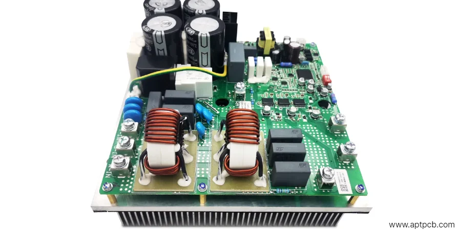
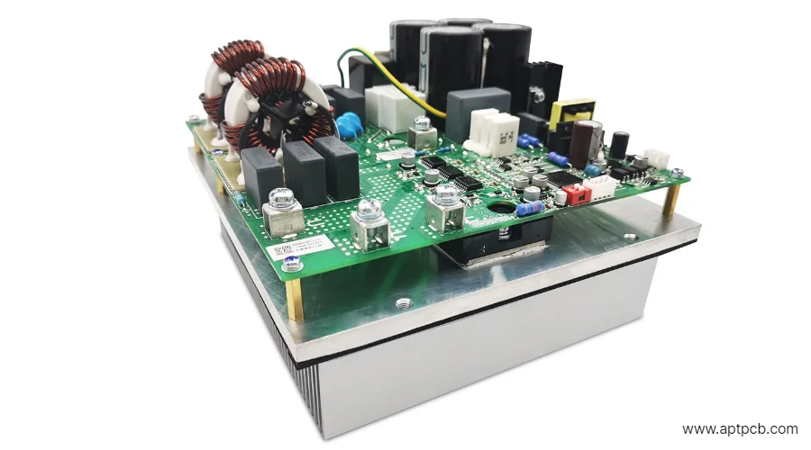
At APTPCB, we manufacture gate driver PCBs with flex-rigid-flex capabilities implementing isolated high-side and low-side drive circuits, desaturation protection, and advanced diagnostic features. Our manufacturing supports two-level, three-level, and multi-level inverter topologies across voltage ranges from 400V industrial drives through 1500V utility-scale solar inverters.
Implementing High-Side and Low-Side Drive
Three-phase inverters require six gate drivers controlling upper and lower switches in each phase leg, with high-side drivers referenced to switching output nodes experiencing hundreds of volts common-mode transients requiring galvanic isolation, proper bootstrap power supplies, or isolated power delivery. Low-side drivers referenced to DC negative rail require simpler implementation but demand coordination with high-side signals preventing shoot-through failures.
At APTPCB, our PCB manufacturing implements robust gate drive architectures ensuring reliable switching control.
Key Gate Drive Design Requirements
High-Side Drive Isolation Methods
- Transformer-coupled gate drive using high-frequency pulse transformers providing galvanic isolation, inherent level shifting, and simple implementation with box build assembly integration
- Optocoupler isolation using high-speed optocouplers transmitting gate signals across isolation barriers maintaining timing accuracy despite common-mode transients
- Capacitive isolation using coreless transformers or isolated gate drivers (Silicon Labs Si823x, ADI ADuM4135) achieving high common-mode transient immunity (>100kV/μs)
- Fiber optic isolation for highest noise immunity applications transmitting optical signals immune to electromagnetic interference
- Bootstrap power supply using bootstrap diodes and capacitors powering high-side drivers from DC bus during each switching cycle
- Isolated DC-DC converters providing continuous power to high-side drivers enabling static operation without bootstrap refresh requirements
Gate Drive Current and Speed
- Peak gate current capability (2-10A) rapidly charging gate capacitance achieving fast turn-on reducing switching losses and voltage overshoot
- Adjustable gate resistance controlling turn-on/turn-off speed balancing switching losses against EMI generation and dv/dt stress
- Split output stages using different resistances for turn-on versus turn-off optimizing switching waveforms independently
- Active gate drive clamping preventing parasitic turn-on from Miller current during opposite switch transitions
- Dead-time control inserting blanking periods between turn-off and turn-on preventing shoot-through where both devices conduct simultaneously
- ICT test validation verifying gate drive circuit connectivity and component values before power-up testing
Layout Optimization
- Minimized gate loop inductance keeping gate drive traces short and wide reducing ringing and voltage overshoot during switching
- Kelvin source connection for MOSFET or IGBT emitter providing clean gate drive reference unaffected by main current path inductance
- Gate resistor placement close to gate terminal minimizing parasitic inductance affecting switching behavior
- Separate power and signal grounds preventing high di/dt currents from coupling into control signals causing false triggering
- Shielding and guard traces isolating high-speed switching signals from sensitive analog measurements or control circuits
- Flying probe testing detecting opens, shorts, and incorrect component placements in complex gate drive layouts
Protection Features
- Desaturation detection monitoring collector-emitter or drain-source voltage detecting short circuits or overcurrent within microseconds
- Active Miller clamp preventing parasitic turn-on during fast dv/dt transients improving reliability in noisy industrial environments
- Undervoltage lockout preventing gate drive operation if supply voltage inadequate ensuring proper switching or preventing undefined states
- Fault status reporting communicating protection events to system controller enabling coordinated shutdown and diagnostics
- Soft shut-down during faults controlling gate discharge preventing secondary failures from inductive kickback
- SPI inspection verifying solder paste volume on critical protection circuit components
PCB Construction
- Multi-layer stackup separating high-speed gate signals, analog measurements, and power distribution minimizing crosstalk
- Controlled impedance routing for high-speed communication interfaces between controller and gate drivers
- Proper creepage and clearance distances maintaining isolation barriers per UL, VDE, or IEC standards (typically 6-8mm for reinforced isolation)
- High-voltage PCB materials with enhanced tracking resistance preventing surface breakdown under contamination
- Thermal management for gate drive ICs and resistors dissipating watts during high-frequency switching
- Conformal coating protecting circuits from humidity and contamination in harsh industrial environments
Reliable Gate Drive Implementation
Through optimized gate drive circuits, proper isolation implementation, and validated PCB manufacturing processes coordinated with our communication equipment expertise, APTPCB delivers gate driver PCBs achieving fast, reliable switching control supporting industrial motor drives, renewable energy inverters, and traction applications.
Achieving Fast Switching Performance
Modern inverters use switching frequencies from 4-20kHz (high-power industrial drives, grid inverters) through 50-100kHz (compact motor drives, solar microinverters) balancing switching losses against filter size and audible noise. Fast switching requires careful gate drive design minimizing parasitic inductance, optimizing gate resistance, and controlling dv/dt and di/dt during transitions preventing electromagnetic interference, voltage overshoot, or false triggering.
APTPCB implements high-frequency optimized layouts supporting fast switching requirements.
Key Fast Switching Techniques
Parasitic Inductance Minimization
- Gate drive PCB layout keeping power loop areas minimal reducing inductance causing voltage spikes during turn-off
- Low-inductance capacitor placement locating DC bus capacitors close to IGBT/MOSFET modules minimizing commutation loop inductance
- Multi-layer PCB with power planes providing low-inductance current return paths
- Proper via placement and density optimizing current distribution and return paths
- Component selection prioritizing low-inductance packages (surface-mount, low-profile devices) over through-hole alternatives
- Simulation and measurement validating inductance reduction techniques achieving specified switching performance
Gate Resistance Optimization
- Gate resistor selection balancing turn-on speed (lower resistance = faster) against overshoot, ringing, and EMI
- Turn-off resistance controlling di/dt during turn-off preventing excessive voltage spikes from stray inductance
- Active gate drive circuits dynamically adjusting gate current during switching optimizing waveforms
- Split resistor configurations using different values for turn-on and turn-off independently optimizing each transition
- Temperature compensation accounting for gate threshold voltage shifts maintaining consistent switching across temperature ranges
- Testing across production validating consistent switching performance despite component tolerances
dv/dt and di/dt Control
- Controlled switching speed preventing excessive dv/dt causing capacitive coupling and EMI generation
- Snubber circuits limiting voltage overshoot and ringing during turn-off protecting semiconductors
- Soft-switching techniques (zero-voltage switching, zero-current switching) eliminating hard transitions reducing losses and stress
- Gate drive timing coordination ensuring proper dead-time preventing shoot-through while minimizing body diode conduction
- Load-dependent optimization adjusting switching speed based on current level balancing losses and stress
- Drone UAV applications requiring compact high-frequency designs benefiting from optimized switching techniques
Providing Galvanic Isolation
High-side gate drivers operate at output node potential floating hundreds of volts above ground reference requiring galvanic isolation between low-voltage control electronics and high-voltage power stage. Isolation barriers must withstand continuous common-mode voltage, transient overvoltages, and high dv/dt (>50kV/μs) while maintaining signal integrity and meeting safety standards (UL, VDE, IEC 60747-5-5) for reinforced isolation protecting personnel and equipment.
APTPCB implements validated isolation techniques ensuring safety and performance.
Key Isolation Implementation
Isolation Technology Selection
- Transformer isolation using pulse transformers providing galvanic barrier with inherent signal transfer
- Optical isolation using high-speed optocouplers rated for >10kV/μs common-mode transient immunity
- Capacitive isolation using iCoupler or similar technology achieving >100kV/μs CMTI in compact packages
- Magnetic isolation combining advantages of transformer and IC integration
- Isolation rating selection (basic, reinforced) based on application safety requirements and standards compliance
- Robotics and industrial automation applications requiring reliable isolation in harsh electrical environments
PCB Isolation Design
- Creepage distance maintaining minimum surface distance between isolated circuits per safety standards
- Clearance distance providing minimum air gap preventing arc-over under transient overvoltages
- Isolation slot routing or cutouts eliminating conductive paths across isolation barriers
- Isolation zone keepouts preventing copper pours, traces, or vias violating isolation requirements
- Layer assignment separating isolated circuits onto different PCB layers with core material providing dielectric barrier
- Testing and validation including hipot testing, partial discharge measurement, and transient immunity verification
Managing Bootstrap Power Supplies
Bootstrap power supplies provide simple, cost-effective power delivery to high-side gate drivers by charging bootstrap capacitors from DC bus through bootstrap diodes during low-side switch conduction. Proper bootstrap design ensures adequate capacitor charging, maintains voltage during high-side conduction, and handles worst-case conditions including maximum duty cycle, startup, and fault scenarios.
APTPCB implements reliable bootstrap circuits supporting demanding operating conditions.
Key Bootstrap Design Requirements
Bootstrap Capacitor Sizing
- Charge storage capacity providing gate drive current and quiescent current during maximum on-time
- Voltage rating withstanding DC bus voltage plus safety margin (typically 2x minimum)
- Low ESR reducing voltage drop during peak gate current draw
- Temperature rating surviving elevated ambient and self-heating from ripple current
- Refresh cycle design ensuring adequate recharge opportunity even at high duty cycles approaching 100%
- Quality inspection screening capacitors for capacitance tolerance and ESR specifications
Bootstrap Diode Selection
- Fast recovery diodes minimizing reverse recovery charge preventing shoot-through during transitions
- Adequate current rating handling bootstrap capacitor charging inrush current
- Reverse voltage rating withstanding full DC bus voltage plus transients
- Forward voltage drop minimizing losses and temperature rise in high-frequency operation
- Package thermal management dissipating power generated during high-frequency charging cycles
- Alternative active bootstrap circuits for applications approaching 100% duty cycle where passive bootstrap insufficient
Implementing Protection and Diagnostics
Gate driver protection circuits detect fault conditions including short circuits, overcurrent, overtemperature, and supply failures triggering safe shutdown preventing catastrophic failures. Diagnostic features report fault conditions to system controller enabling coordinated protection responses, fault logging for maintenance analysis, and predictive algorithms preventing failures before occurrence.
APTPCB manufactures gate driver PCBs with comprehensive protection integration.
Key Protection Features
Desaturation (DESAT) Protection
- Collector/drain voltage monitoring detecting saturation voltage increase indicating short circuit or overcurrent
- Fast response (<2μs) shutting down gate drive before thermal damage occurs
- Blanking time during turn-on ignoring high voltage during normal switching preventing false trips
- Adjustable threshold accommodating different semiconductor types and current levels
- Fault latch or auto-retry operation providing flexibility for application-specific recovery strategies
- Diagnostic reporting communicating fault type and affected phase to system controller
Supply Monitoring and UVLO
- Gate drive supply voltage monitoring ensuring adequate voltage for proper switching
- Undervoltage lockout preventing gate drive operation if supply inadequate
- Overvoltage protection preventing damage from supply transients or failures
- Redundant supplies with automatic switching maintaining operation despite single supply failure
- Supply sequencing ensuring proper power-up and power-down preventing undefined states
- BGA reballing repair services supporting long-term gate driver module maintenance
Supporting Motor Drive and Solar Inverters
Gate driver PCBs serve diverse applications including industrial motor drives (variable frequency drives, servo drives), renewable energy (solar inverters, wind turbine converters), electric vehicles (traction inverters, onboard chargers), and grid infrastructure (STATCOM, HVDC) requiring application-specific optimizations in switching frequency, isolation rating, protection features, and environmental specifications.
APTPCB provides flexible manufacturing supporting diverse inverter applications.
Key Application Support
Industrial Motor Drives
- Switching frequencies 4-16kHz balancing motor performance, efficiency, and acoustic noise
- Three-level or multi-level topologies reducing dv/dt stress on motor windings
- Encoder and resolver interfaces integrating position feedback for servo control
- Industrial communication protocols (Profinet, EtherCAT, Modbus) supporting factory automation
- Harsh environment ratings (IP65, conformal coating) surviving factory floor conditions
- 20+ year design life supporting industrial equipment longevity expectations
Solar and Wind Inverters
- Grid-tie synchronization maintaining phase and frequency lock with utility grid
- Maximum power point tracking (MPPT) optimizing energy harvest from solar panels or wind turbines
- Anti-islanding protection detecting grid loss and disconnecting inverter ensuring safety
- High efficiency (>98%) maximizing energy yield and reducing thermal management requirements
- String or central inverter configurations supporting utility-scale installations
- 25+ year reliability matching solar panel warranties through robust component selection
Through application-optimized designs, flexible manufacturing capabilities, and comprehensive support services, APTPCB enables inverter manufacturers deploying reliable gate driver solutions across diverse motor drive, renewable energy, and industrial power conversion markets worldwide.