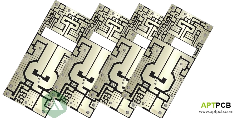
Microwave PCB manufacturing represents the highest precision tier of circuit board fabrication, producing boards for applications operating from 3 GHz through 300 GHz where manufacturing tolerances directly translate to electrical performance. At 77 GHz, trace width variations of 0.5 mil affect impedance measurably, gap dimension changes of 0.3 mil shift filter response, and material property variations alter phase velocity—making precision manufacturing essential for functional circuits.
This guide covers the critical aspects of microwave PCB manufacturing—dimensional control, material handling, via technologies, surface quality, and validation—providing the foundation for successful microwave circuit fabrication.
Mastering Ultra-Precision Dimensional Control
Dimensional precision in microwave PCB manufacturing directly determines electrical performance with tolerances far tighter than conventional fabrication.
Trace Width Requirements
At millimeter-wave frequencies, impedance sensitivity to trace width is acute. For a 50Ω microstrip on typical substrate at 77 GHz:
- Nominal trace width: approximately 10 mils
- ±0.5 mil width variation → ±5% impedance change
- This 5% shift degrades return loss from -20 dB to approximately -15 dB
Achieving this accuracy requires:
- Optimized photolithography with documented exposure parameters
- Controlled etching with statistical process monitoring
- Etch compensation factors validated for specific material/copper combinations
- Measurement systems capable of ±0.1 mil resolution
Gap Dimension Control
Gap dimensions between coupled structures determine electromagnetic coupling:
Edge-Coupled Filters:
- Filter bandwidth proportional to coupling gap
- ±0.5 mil tolerance on 4-mil gap → ±12.5% bandwidth variation
- Center frequency shifts with resonator length accuracy
Directional Couplers:
- Coupling varies approximately 0.4 dB per mil of gap change
- Gap uniformity along coupled length affects directivity
Manufacturing processes must achieve gap consistency within ±0.5 mil or better.
Layer Registration
Registration between layers affects:
- Via connection to traces (misalignment creates discontinuities)
- Multilayer distributed structure alignment
- Ground via fence positioning
For multilayer microwave constructions, registration within ±2 mil ensures proper feature alignment.
Key Dimensional Control Achievements
- Trace Width Precision: ±0.5 mil tolerance through optimized imaging and etch control.
- Gap Dimension Accuracy: Coupled structures within ±0.5 mil for designed coupling.
- Dielectric Thickness Control: Lamination achieving thickness within ±0.5 mil.
- Registration Accuracy: Layer alignment within ±2 mil.
- Panel Uniformity: Consistent dimensions across production panel through rigorous quality systems.
- Lot Consistency: Statistical process control maintaining capability across production.
Handling Specialized Microwave Materials
Microwave PCB manufacturing requires expertise with materials behaving very differently from standard FR-4.
PTFE Processing
PTFE-based materials like Rogers RT/duroid provide lowest loss but present significant challenges:
Drilling:
- Soft, thermoplastic nature causes material smearing
- Smear blocks plating adhesion if not properly removed
- Parameters typically 40-60% of FR-4 speeds
- Specialized geometries with increased relief angles
Desmear:
- Plasma processing removes residual smear
- Process parameters (power, time, gas mixture) material-specific
- Verification through cross-section or pull testing
Surface Preparation:
- Low surface energy requires activation for plating adhesion
- Sodium naphthalenide etching chemically modifies surface
- Plasma treatment provides physical and chemical activation
Ceramic-Filled Materials
Ceramic fillers create abrasive conditions:
- Tool wear 2-5× faster than standard materials
- Diamond-coated or specialized carbide tools required
- Tool change frequency increases manufacturing time and cost
- Edge quality requires attention during routing
Lamination Adaptation
Different materials require different press cycles:
- PTFE: Extended dwell, controlled ramps, different flow characteristics
- Hybrid stackups: Compatible bonding between dissimilar materials through specialized fabrication processes
- Process documentation captures parameters for each material combination
Implementing Advanced Via Technologies
Via structures in microwave PCBs require technologies minimizing parasitic effects while enabling layer transitions and ground connections.
Back Drilling
Back drilling removes via stubs creating quarter-wave resonances:
Process:
- Standard through-hole fabrication first
- Controlled-depth drilling from board surface removes stub
- Depth accuracy within ±4 mils ensures complete removal with margin
Design Considerations:
- Minimum remaining stub typically 6-8 mils
- Resonance frequency shifts above operating range
- Cost addition typically 10-15%
Laser Microvias
Laser drilling creates small vias for HDI microwave constructions:
- Diameters below 100 μm achievable
- Lower inductance than mechanical drilling
- Blind vias eliminate stub effects entirely
- Stacked or staggered configurations span multiple layers
Via Fencing
Ground via fences create electromagnetic barriers:
- Via spacing ≤ λ/20 at operating frequency for effective shielding
- At 30 GHz, this means ≤0.5mm spacing
- Consistent diameter and plating throughout arrays essential
- Position accuracy maintains fence integrity
Key Via Technology Implementations
- Back Drill Precision: Depth control within ±4 mils ensuring complete stub removal.
- Microvia Formation: Laser drilling achieving consistent small-diameter vias.
- Blind Via Structures: Layer-specific connections without stub resonance.
- Via Fence Implementation: Consistent arrays providing electromagnetic isolation.
- Plating Quality: Uniform copper throughout via structures.
- Position Accuracy: Via placement within ±2 mil for designed feature connection.
Achieving Surface Quality for Microwave Performance
Surface quality affects conductor losses and processing compatibility. At microwave frequencies, current flows in the surface skin layer making surface characteristics critical.
Copper Surface Roughness
The relationship between roughness and skin depth determines loss impact:
| Frequency | Skin Depth | Roughness Impact |
|---|---|---|
| 1 GHz | 2.1 μm | Moderate if Rz > 2 μm |
| 10 GHz | 0.66 μm | Significant if Rz > 1 μm |
| 77 GHz | 0.24 μm | Critical—smooth copper essential |
Achieving low roughness requires:
- Low-profile copper foil selection
- Plating parameters avoiding nodular growth
- Controlled etching maintaining surface quality
Trace Edge Quality
Edge roughness affects impedance uniformity:
- Irregular edges create local impedance variations
- Rough edges add to conductor loss
- Etching optimization produces smooth, consistent edges
Key Surface Quality Factors
- Copper Roughness Control: Foil selection and plating for low Rz.
- Edge Definition: Etching producing smooth trace edges.
- Cleanliness Standards: Surface preparation for subsequent processing.
- Visual Standards: Appearance criteria for high-reliability applications.
Validating Microwave Performance Through Testing
Microwave PCB manufacturing requires comprehensive testing confirming dimensional accuracy and electrical performance.
Vector Network Analysis
S-parameter characterization across frequency:
- S11 (return loss): Confirms impedance matching
- S21 (insertion loss): Quantifies signal attenuation
- Phase measurements: Verify electrical length accuracy
Calibration at defined reference planes essential for accurate results.
TDR Impedance Testing
Time Domain Reflectometry profiles impedance along transmission lines:
- Identifies impedance variations and their locations
- Non-destructive testing using production coupons
- Correlates to design predictions for process validation
Dimensional Verification
Precision measurement systems confirm:
- Trace widths within ±0.5 mil tolerance
- Gap dimensions for coupled structures
- Layer registration accuracy
Statistical analysis tracks process capability and identifies trends.
Key Microwave Testing Protocols
- S-Parameter Characterization: Network analysis confirming transmission and reflection.
- TDR Impedance Profiling: Impedance measurement identifying variations.
- Dimensional Verification: Precision measurement confirming geometry.
- Material Documentation: Certification and traceability.
- Cross-Section Analysis: Internal structure verification through comprehensive quality inspection.
Supporting Demanding Microwave Applications
Microwave PCB manufacturing serves applications where performance at elevated frequencies determines system success.
Application Areas
Radar Systems: Phase control accuracy determines beam pointing and target resolution. Manufacturing consistency across phased array modules enables system calibration.
Satellite Communications: Insertion loss directly impacts link budget. Low-loss fabrication extends communication range or reduces transmitter power.
5G Millimeter-Wave: The telecommunications industry requires 28 GHz and 39 GHz infrastructure boards with consistent performance across high volumes.
Automotive Radar: The automotive sector demands 77 GHz boards meeting both performance and automotive quality requirements at competitive cost.
For comprehensive manufacturing information, see our guide on high frequency PCB manufacturing.