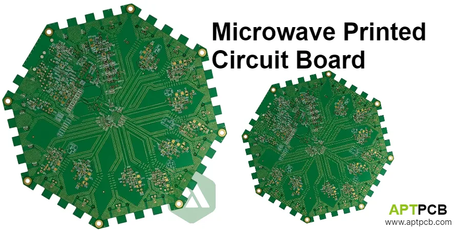
A microwave printed circuit board operates at frequencies from 3 GHz through 300 GHz where wavelengths become comparable to circuit feature dimensions and electromagnetic wave behavior completely dominates design and manufacturing requirements. At 10 GHz, wavelength in a typical substrate is approximately 15mm; at 77 GHz, it shrinks to about 2mm—comparable to trace widths and via dimensions.
These boards demand ultra-low loss materials, exceptional dimensional precision, and advanced fabrication processes to support radar systems, satellite communications, 5G millimeter-wave networks, and scientific instrumentation where fractions of a decibel in loss or degrees in phase determine system capability.
Selecting Ultra-Low Loss Material Systems
Material selection at microwave frequencies directly determines achievable system performance with impact far exceeding lower frequency applications. The relationship between insertion loss and dissipation factor becomes increasingly critical:
Loss (dB/inch) ≈ 2.3 × f(GHz) × √Dk × Df
At 30 GHz, a material with Df=0.004 exhibits approximately 0.5 dB/inch loss, while Df=0.001 reduces this to 0.13 dB/inch—a 4× improvement that can represent several dB over typical interconnect lengths.
PTFE-Based Laminates
PTFE-based laminates provide the lowest dielectric loss essential for microwave transmission lines. Rogers RT/duroid materials achieve Df below 0.001 at 10 GHz—ten times better than standard RF materials and one hundred times better than FR-4.
Key PTFE substrate options:
- RT/duroid 5880: Dk=2.2, Df=0.0009—lowest loss, suitable to 77+ GHz
- RT/duroid 6002: Dk=2.94, Df=0.0012—improved dimensional stability
- RO3003: Dk=3.0, Df=0.0013—ceramic-filled for thermal stability
Ceramic-Filled PTFE Materials
Ceramic-filled PTFE materials like Rogers RO3000 series combine low loss with exceptional dielectric constant stability across temperature:
- Dk variation typically <50 ppm/°C vs >200 ppm/°C for unfilled PTFE
- Stable performance from -50°C to +150°C
- Improved thermal conductivity (0.5 W/m·K vs 0.2 W/m·K for unfilled PTFE)
This stability ensures consistent impedance and electrical length despite environmental temperature variations—critical for outdoor installations, automotive systems, and aerospace applications.
Liquid Crystal Polymer (LCP)
LCP materials offer unique advantages for millimeter-wave frequencies:
- Very low moisture absorption (<0.04%) preventing Dk shifts in humid environments
- Stable properties through 110 GHz
- Suitable for flexible/rigid-flex constructions
Key Material Selection Criteria
- Frequency-Matched Loss: Df below 0.002 for frequencies above 20 GHz, below 0.001 for millimeter-wave applications.
- Dk Stability: Dielectric constant variation within ±2% across operating temperature range ensuring predictable impedance.
- Moisture Resistance: Low water absorption (<0.1%) preventing Dk shifts—critical for outdoor and marine installations.
- Thermal Performance: Stable properties through assembly (260°C reflow) and operating thermal cycles.
- Processing Compatibility: Material behavior during drilling, plating, and lamination compatible with manufacturing capabilities. See specialized fabrication techniques.
- Copper Foil Integration: Low-profile copper (Rz < 2 μm) reducing surface roughness contribution to conductor loss.
Achieving Dimensional Precision for Microwave Structures
Microwave circuit dimensions directly determine electrical performance with tolerances far tighter than lower frequency applications. The relationship between physical and electrical parameters becomes increasingly sensitive at higher frequencies.
Trace Width Impact
Trace width determines characteristic impedance. For a 50Ω microstrip on 5-mil RT/duroid 5880:
- Nominal trace width: approximately 15 mils
- ±0.5 mil width variation → ±3% impedance change
- At 77 GHz, this translates to measurable return loss degradation
Manufacturing must achieve width tolerance within ±0.5 mil (±12.7 μm) through optimized photolithography, carefully controlled etching, and statistical process monitoring.
Gap Dimensions
Gap dimensions between coupled structures critically affect coupling coefficient:
- Edge-coupled filter bandwidth varies approximately 2× gap tolerance percentage
- 4-mil gap with ±0.5 mil tolerance → ±12.5% bandwidth variation
- Directional coupler coupling varies 0.3-0.5 dB per mil of gap change
Gap tolerances of ±0.5 mil or better are typically required for predictable filter and coupler performance.
Layer Registration
At microwave frequencies, layer-to-layer registration affects:
- Via connection to traces (misalignment creates discontinuities)
- Alignment of multilayer distributed structures
- Ground via positioning for via fences
Registration within ±2 mil ensures vias connect intended features and multilayer structures maintain designed relationships.
Key Dimensional Control Requirements
- Trace Width Tolerance: ±0.5 mil accuracy through photolithography optimization and etch process control.
- Gap Dimension Control: Coupled structure spacing within ±0.5 mil ensuring designed coupling coefficients.
- Dielectric Thickness: Lamination processes controlling thickness within ±0.5 mil for predictable impedance and phase velocity.
- Registration Accuracy: Layer alignment within ±2 mil ensuring via positioning and multilayer structure alignment.
- Edge Definition: Smooth, consistent trace edges (edge roughness < trace width/20) minimizing loss and impedance variations.
- Panel Uniformity: Consistent dimensions across production panel through rigorous quality control.
Implementing Advanced Microwave Structures
Microwave circuits employ specialized structures implemented directly in PCB traces where geometry precisely determines electromagnetic response.
Coupled-Line Filters
Edge-coupled bandpass filters use parallel transmission line resonators:
- Resonator length ≈ λ/4 at center frequency determines passband location
- Gap between resonators determines bandwidth and response shape
- Typical 3-5 resonator designs achieve 20-40 dB out-of-band rejection
Design example: 10 GHz bandpass filter on Dk=3 substrate requires approximately 4mm resonator length with 4-8 mil coupling gaps depending on desired bandwidth.
Branch-Line Couplers
Branch-line (quadrature) hybrids create 90° phase split between ports:
- Four quarter-wave transmission line sections
- 3 dB split with 90° phase difference between coupled and through ports
- Used in balanced amplifiers, I/Q modulators, and antenna feed networks
Performance sensitivity: ±1° phase accuracy requires ±0.3% length tolerance.
Wilkinson Dividers
Wilkinson power dividers provide equal-split with isolation:
- Quarter-wave 70.7Ω sections (for 50Ω system)
- 100Ω thin-film resistor between outputs
- Achievable performance: >20 dB isolation, <0.3 dB imbalance
Patch Antennas
Patch antenna arrays integrate directly on microwave PCBs:
- Patch dimensions ≈ λ/2 at resonant frequency
- Substrate Dk determines patch size and bandwidth
- Lower Dk provides wider bandwidth but larger patches
Managing Thermal Challenges in Microwave Systems
Microwave power amplifiers operating at 30-50% efficiency convert substantial input power to heat. A 10W PA at 40% efficiency dissipates 15W—concentrated in devices smaller than 5mm square.
Thermal Via Design
Thermal via arrays beneath power devices provide critical heat paths:
- Typical design: 0.3mm diameter vias on 0.6mm pitch
- Via fill options: solid copper, thermally conductive paste
- Achievable thermal resistance: 10-20°C/W from device to board bottom
Design trade-off: Dense vias improve thermal performance but can affect RF grounding if via inductance becomes significant.
Heavy Copper Construction
Heavy copper layers enhance thermal spreading:
- 2 oz copper provides 2× thermal spreading vs 1 oz
- 4 oz copper enables high-current DC distribution for PA bias
- See heavy copper PCB capabilities
Metal Core Options
For highest power applications:
- Aluminum core: 1-2 W/m·K thermal conductivity, good cost
- Copper core: 385 W/m·K, best thermal but higher cost
- Dielectric isolation layer typically 75-150 μm
Key Thermal Management Approaches
- Thermal Via Optimization: Via patterns balancing thermal resistance with RF performance.
- Copper Weight Selection: Heavy copper for thermal spreading, considering manufacturing process impacts.
- Metal Core Integration: Direct thermal paths for high-power stages exceeding conventional PCB thermal capacity.
- Interface Material Provisions: Board features accommodating thermal compound or pad application.
- Thermal Modeling: Finite element analysis predicting temperature distribution before fabrication.
- Component Derating: Design margins ensuring junction temperatures remain within ratings under worst-case conditions.
Ensuring Environmental Reliability
Microwave systems often operate in extreme environments requiring robust construction.
Temperature Cycling
Thermal cycling creates stress from CTE mismatch:
- Copper: 17 ppm/°C
- PTFE: 70-100 ppm/°C (unfilled), 20-40 ppm/°C (ceramic-filled)
- FR-4: 14-17 ppm/°C in-plane
Solutions include ceramic-filled materials reducing CTE mismatch, proper via design accommodating Z-axis expansion, and high-Tg material selection for dimensional stability.
Moisture Resistance
Moisture affects dielectric constant:
- Water Dk ≈ 80 vs substrate Dk ≈ 2-4
- 0.1% moisture absorption can shift Dk by 1-2%
- Critical for outdoor, marine, and tropical installations
PTFE materials inherently resist moisture (<0.02% absorption); other materials require careful selection and potential conformal coating.
Key Environmental Protection Requirements
- Thermal Cycling Capability: Construction surviving specified cycles (-55°C to +125°C typical for military) without delamination.
- Moisture Resistance: Material selection and protection preventing Dk shifts in humid environments.
- Vibration Tolerance: Mechanical design withstanding specified vibration spectra without solder joint failure.
- Outgassing Compliance: NASA ASTM E595 compliance for space applications.
- Altitude Performance: Consideration of reduced cooling and corona onset at high altitude.
- Long-Term Stability: Construction ensuring consistent performance across 10-15 year product lifetimes.
Validating Microwave Performance
Microwave printed circuit boards require sophisticated testing confirming performance across operating frequency ranges.
Vector Network Analysis
S-parameter characterization using vector network analyzer (VNA):
- S11: Return loss (impedance match quality)
- S21: Insertion loss (transmission efficiency)
- S12, S22: Reverse parameters for complete characterization
Calibration to reference planes at connector interfaces or probe points is essential for accurate measurements.
Time Domain Analysis
TDR (Time Domain Reflectometry) identifies impedance discontinuities:
- Locates variations along transmission lines
- Spatial resolution approximately 1mm with 50 ps rise time
- Useful for identifying manufacturing variations
Key Microwave Testing Requirements
- Network Analysis: S-parameter characterization across operating frequency confirming specifications.
- TDR Verification: Impedance profiling identifying variations and validating controlled impedance achievement.
- Dimensional Measurement: Precision inspection confirming trace geometry meets design tolerances.
- Material Certification: Traceability linking boards to material lot properties.
- Environmental Testing: Temperature cycling and humidity exposure validating reliability.
- Cross-Section Analysis: Microsection examination through comprehensive quality inspection.
For detailed manufacturing information, see our guide on high frequency PCB manufacturing.