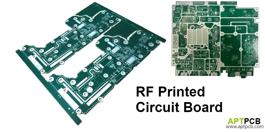
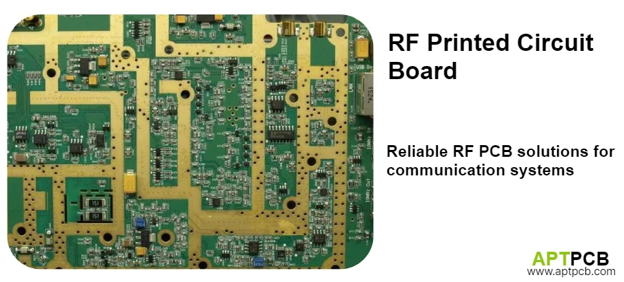
An RF printed circuit board translates radio frequency circuit designs into physical implementations where PCB traces become integral circuit elements rather than simple interconnects. Unlike digital boards where traces primarily connect components, RF boards require traces functioning as precision transmission lines, impedance matching networks, and distributed filter elements.
This guide covers the essential RF PCB design principles—transmission line implementation, impedance matching, shielding strategies, and distributed circuit elements—providing engineers with foundational knowledge for successful RF design and manufacturing.
Mastering Transmission Line Implementation
Every trace in an RF printed circuit board behaves as a transmission line characterized by impedance, propagation velocity, and attenuation. These parameters determine how effectively signals transfer from source to load, with mismatches causing reflections that degrade system performance.
Characteristic Impedance
Characteristic impedance (Z₀) represents the ratio of voltage to current along an infinitely long transmission line—determined entirely by geometry and materials, not by what's connected at either end. For microstrip lines, Z₀ depends on:
- Trace width: Wider traces = lower impedance (roughly logarithmic relationship)
- Dielectric thickness: Greater spacing to ground = higher impedance
- Dielectric constant: Higher Dk = lower impedance (approximately 1/√Dk relationship)
- Copper thickness: Minor effect, typically 2-3% variation over practical range
Most RF systems standardize on 50Ω impedance, though 75Ω appears in video and cable television applications. Maintaining consistent impedance throughout signal paths minimizes reflections at every point along the transmission line.
Phase Velocity and Electrical Length
Phase velocity determines physical trace length required for specific electrical length—critical for RF circuits using quarter-wave transformers, delay lines, and phase-matched networks.
Signals propagate at approximately 50-70% of light speed depending on effective dielectric constant:
v = c / √Dk_effective
For microstrip on Dk=4 substrate, effective Dk ≈ 3, giving velocity ≈ 1.7×10⁸ m/s. A quarter wavelength at 2.4 GHz is approximately 18mm physical length on such a substrate.
Insertion Loss
Insertion loss accumulates along transmission line length, combining:
- Conductor loss: From skin effect resistance, proportional to √frequency, minimized by smooth copper and wider traces
- Dielectric loss: From substrate dissipation factor, proportional to frequency, minimized by low-Df materials
Total loss typically ranges from 0.1 dB/inch at 1 GHz to 0.5 dB/inch at 10 GHz for quality RF materials, higher for standard FR-4.
Key Transmission Line Design Requirements
- Impedance Consistency: Trace geometry maintaining characteristic impedance within ±5% tolerance throughout entire signal path including bends and width transitions.
- Phase Accuracy: Electrical length control enabling quarter-wave structures and phase-sensitive distributed elements—typically ±1° phase tolerance requires ±0.3% length accuracy.
- Loss Budget Management: Material selection and path length optimization keeping total insertion loss within system budget, typically 1-3 dB allocation for PCB interconnect.
- Discontinuity Minimization: Smooth transitions at bends (use mitered corners or curves rather than 90° angles), via connections, and component interfaces.
- Reference Plane Integrity: Continuous ground planes beneath RF traces through multilayer construction.
- Manufacturing Alignment: Geometry specifications within fabrication process capabilities—trace widths above 4 mils, gaps above 4 mils for standard processes.
Implementing Distributed Matching Networks
RF circuits require impedance matching between sources, transmission lines, and loads for maximum power transfer. RF printed circuit boards often implement matching networks directly in PCB traces, eliminating discrete components while achieving precise, repeatable transformation ratios.
Quarter-Wave Transformers
Quarter-wave transformers use transmission line sections of quarter-wavelength electrical length to transform impedance. The transformation follows:
Z_in = Z₀² / Z_load
A 50Ω system matching to 100Ω load requires 70.7Ω quarter-wave section (√(50×100)). These structures demand both accurate electrical length and precise characteristic impedance—manufacturing tolerance directly determines achievable VSWR.
For example, achieving VSWR < 1.5:1 over 10% bandwidth requires impedance accuracy within ±5% and length accuracy within ±2%.
Tapered Transmission Lines
Tapered lines provide gradual impedance transitions achieving broadband matching with lower reflection than abrupt step changes. Common profiles include:
- Linear taper: Simple to design, moderate performance
- Exponential taper: Improved bandwidth for given length
- Klopfenstein taper: Optimal ripple/bandwidth trade-off for specified length
Taper implementation requires smooth trace width variation accurately following designed profile—typically requiring ±0.5 mil manufacturing tolerance on width.
Stub Matching
Stub matching uses open or short-circuit transmission line stubs providing reactive susceptance for impedance matching. Stub length determines susceptance magnitude:
- Open stub: Acts as capacitor when shorter than λ/4, inductor when longer
- Shorted stub: Opposite behavior to open stub
Single-stub matching can match any load with proper stub length and position. Double-stub configurations offer adjustment flexibility but narrower bandwidth.
Key Matching Network Implementation Factors
- Electrical Length Accuracy: Physical dimensions achieving required electrical length accounting for effective Dk—verify through simulation before fabrication.
- Impedance Control: Trace geometry achieving intermediate impedance values (e.g., 70.7Ω, 35.4Ω) within tolerance.
- Bandwidth Consideration: Single-section quarter-wave transformers provide approximately 20% bandwidth for VSWR < 2:1; multi-section designs extend bandwidth.
- Loss Impact: Each matching section adds insertion loss—typically 0.1-0.3 dB per quarter-wave section depending on material.
- Tuning Provisions: Design features enabling post-fabrication optimization for prototypes—tuning stubs, component pads near trace ends.
- Repeatability: Manufacturing consistency ensuring matching performance across production volumes.
Engineering Shielding and Isolation
RF printed circuit boards often contain both sensitive receivers and powerful transmitters requiring careful isolation to prevent interference. Achieving required isolation—often 60-80 dB between transmit and receive—demands coordinated application of grounding, shielding, and layout compartmentalization.
Ground Plane Integrity
Ground plane integrity fundamentally determines isolation and signal quality:
- Return currents flow directly beneath signal traces within approximately 3 trace-widths
- Slots or gaps force return currents to detour, creating inductance and radiation
- Even 10-mil slots can increase path inductance by 1-2 nH, causing measurable impedance discontinuity
RF designs prioritize uninterrupted reference planes even when this significantly complicates routing on adjacent layers.
Via Fence Isolation
Via fences create electromagnetic barriers between circuit sections using closely-spaced ground vias:
- Via spacing should be ≤ λ/20 at highest operating frequency for effective shielding
- At 10 GHz (λ ≈ 15mm in substrate), via spacing should be ≤ 0.75mm
- Via rows provide 20-40 dB isolation depending on spacing and via count
Shield Can Integration
Surface-mount shield cans provide additional isolation for critical sections:
- Typical isolation improvement: 30-50 dB at frequencies below can resonance
- Requires dense via perimeter (same λ/20 spacing rule) for effective grounding
- Internal compartments can separate stages within single shield
Key Isolation Engineering Considerations
- Return Path Continuity: Uninterrupted ground planes beneath all RF traces—route digital signals on other layers rather than cutting RF ground.
- Via Fence Design: Ground via rows with spacing appropriate for operating frequency creating electromagnetic boundaries.
- Shield Can Accommodation: Footprint patterns enabling surface-mount can attachment with proper ground connection density.
- Compartmentalization Strategy: Board layout organizing functional sections—LNA, PA, oscillator, digital—with physical separation and electromagnetic barriers.
- Layer Stack Contribution: Ground planes positioned between RF and digital sections through HDI construction techniques.
- Verification Planning: Test provisions enabling isolation measurement confirming shielding effectiveness meets requirements.
Optimizing Component Placement and Interconnection
RF component placement significantly impacts circuit performance through parasitic element contribution, electromagnetic coupling paths, and thermal interactions. Every millimeter of trace adds inductance; every pad contributes capacitance; every via introduces impedance discontinuity.
Parasitic Minimization
At RF frequencies, parasitics that are negligible in low-frequency design become dominant:
- Trace inductance: Approximately 1 nH/mm for typical microstrip
- Via inductance: 0.5-1.5 nH per via depending on geometry
- Pad capacitance: 0.1-0.5 pF depending on size and substrate Dk
These parasitics shift circuit response from design targets—a 1 nH parasitic inductance represents 6.3Ω reactance at 1 GHz. Critical RF components require immediate, direct connections with ground vias adjacent to ground terminals providing low-inductance return paths.
Thermal Integration
Thermal management addresses heat dissipation from power amplifiers, regulators, and other dissipative components:
- Thermal vias beneath components conduct heat to inner copper planes
- Via placement must not compromise RF grounding or introduce coupling
- Heavy copper layers provide enhanced thermal spreading for high-power sections
Key Placement Optimization Factors
- Interconnect Minimization: Shortest possible trace lengths connecting RF components—each mm eliminated removes approximately 1 nH inductance.
- Ground Via Proximity: Ground connections within one pad width (≤0.5mm) of component ground terminals.
- Thermal Path Integration: Heat dissipation provisions coordinated with RF grounding—thermal vias can double as ground vias with proper placement.
- Coupling Avoidance: Physical separation of 10× trace width minimum between high-level outputs and sensitive inputs.
- Test Access: Probe point locations for tuning and measurement without excessive parasitic loading.
- Assembly Compatibility: Component spacing meeting automated assembly equipment requirements (typically ≥0.5mm between components).
Implementing Distributed Circuit Elements
RF printed circuit boards implement filters, couplers, dividers, and other circuits directly in PCB traces, eliminating discrete components while achieving precise, repeatable response characteristics. These distributed elements depend entirely on PCB geometry and material properties.
Edge-Coupled Filters
Edge-coupled bandpass filters use parallel transmission line resonators with controlled coupling gaps:
- Gap dimensions of 4-10 mils determine bandwidth and response shape
- Gap tolerance directly impacts bandwidth—±0.5 mil variation can shift bandwidth 10-20%
- Resonator length determines center frequency—electrical quarter-wavelength at center frequency
Wilkinson Power Dividers
Wilkinson dividers provide equal-split power division with isolation between output ports:
- Quarter-wave transmission line sections at 70.7Ω (for 50Ω system)
- Termination resistor (100Ω) between outputs provides isolation
- Achieves 20+ dB isolation, <0.5 dB amplitude imbalance across 20% bandwidth
Branch-Line Couplers
Branch-line couplers create quadrature hybrids providing 90° phase split:
- Four quarter-wave sections forming square or rectangular structure
- Enables balanced amplifier configurations and single-sideband systems
- Requires ±1° phase accuracy, achieved with ±0.3% length tolerance
Key Distributed Element Requirements
- Dimensional Accuracy: Feature geometry within tolerances determined by sensitivity analysis—typically ±0.5 mil for gap-critical structures.
- Material Consistency: Stable Dk ensuring designed electrical length and impedance throughout operating frequency and temperature range.
- Copper Quality: Smooth surfaces (Rz < 3 μm) minimizing conductor loss contribution.
- Process Capability: Element dimensions achievable within demonstrated manufacturing tolerances.
- Test Verification: Measurement provisions (probe pads, connector launches) confirming distributed element response.
- Repeatability: Statistical process control ensuring consistent performance across production volumes.
Achieving Manufacturing Success
RF printed circuit board success requires close partnership between design and manufacturing. Early manufacturing engagement identifies potential issues before they become costly redesign problems.
Design for Manufacturability
DFM analysis should evaluate:
- Trace widths and gaps against process capability (typically ≥4 mil for standard processes)
- Impedance tolerances against demonstrated manufacturing capability (±10% standard, ±5% with enhanced control)
- Material availability and lead time for specified laminates
- Via structures matching drilling and plating capabilities
Quality Validation
Quality validation must address RF-specific parameters:
- Impedance verification: TDR measurement on production coupons
- Dimensional inspection: Trace width and gap measurement
- Material certification: Dk and Df verification against specifications
- S-parameter testing: Return loss and insertion loss for critical paths
Functional testing capabilities validate complete RF assemblies meet system-level specifications.
For comprehensive manufacturing information, see our guide on high frequency PCB manufacturing.