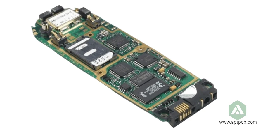
Smartphone PCB assemblies integrate application processors, memory, RF transceivers, power management, cameras, and sensors into ultra-dense 8-16 layer HDI boards measuring 70x140mm requiring 50μm trace widths, via-in-pad construction, and laser-drilled microvias supporting flagship devices processing 5G signals, 4K video, and AI workloads while managing 5-15W thermal dissipation across consumer flagship phones, rugged industrial devices, and mid-range platforms demanding reliable operation through 2-5 year lifecycles surviving millions of charge cycles, temperature extremes, and daily handling stress.
At APTPCB, we deliver specialized smartphone assembly services implementing advanced HDI construction, high-speed signal routing, and comprehensive testing with box build assembly integration. Our capabilities support budget devices requiring cost optimization through flagship platforms demanding cutting-edge 3nm processors, 200MP cameras, and sub-6GHz 5G with validated manufacturing ensuring yield and reliability.
Achieving Extreme Component Density in Thin Form Factors
Modern smartphones pack 1000+ components including multi-die SoCs, LPDDR5 memory, UFS storage, RF front-ends, and PMICs onto PCBs measuring just 1.0-1.4mm thickness while maintaining electromagnetic compatibility and thermal management. Component density reaching 15-20 parts/cm² requires advanced assembly techniques handling 0.35mm BGAs, 01005 passives, and wafer-level packages while managing thermal expansion mismatches and achieving first-pass yields >95%. Inadequate density optimization forces thicker devices reducing market appeal, limits battery capacity affecting runtime, or compromises RF performance impacting network connectivity — directly impacting product competitiveness, user satisfaction, and market success in highly competitive mobile markets.
At APTPCB, our manufacturing implements advanced assembly techniques achieving flagship-level component density and reliability.
High-Density Assembly Implementation Techniques
- Any-Layer HDI Construction: 8-16 layer stackups with 2-3 build-up layers per side enabling via-in-pad for BGAs and achieving 50-75μm trace widths with ICT test electrical validation.
- Stacked Package Integration: Package-on-package assembly stacking LPDDR5 memory on application processors reducing footprint 40% while managing thermal interfaces.
- Ultra-Fine-Pitch Assembly: Precision placement handling 0.35mm pitch BGAs and 01005 passive components with reflow profiles optimized for thin PCBs preventing warpage.
- Via-in-Pad Technology: Filled and plated microvias within BGA pads enabling direct routing eliminating dogbone traces saving precious routing space.
- Sequential Lamination: Build-up layer processing enabling complex via structures and high routing density supporting advanced processor packages.
- Advanced Inspection: High-resolution AOI and 2D/3D X-ray inspection validating solder joints under dense component populations through flying probe testing for rapid debugging.
Validated High-Density Manufacturing
By implementing state-of-the-art HDI manufacturing, precision assembly equipment, and comprehensive inspection protocols supported by experienced engineering teams, APTPCB enables smartphone designs achieving industry-leading component density supporting thin form factors, large batteries, and advanced feature integration across flagship and mid-range mobile devices.
Managing Multi-Standard RF and Antenna Integration
Smartphones simultaneously support 5G (sub-6GHz and mmWave), LTE, WiFi 6E/7, Bluetooth 5.3, NFC, and GPS requiring complex RF front-end integration with dozens of filters, switches, and amplifiers coordinated through careful PCB layout, antenna tuning, and electromagnetic compatibility management. RF performance challenges include isolation between transmitters preventing desensitization, antenna efficiency maximizing range while fitting in limited space, and SAR compliance ensuring user safety. Inadequate RF implementation causes poor cellular reception affecting calls and data, WiFi performance degradation frustrating users, or SAR test failures preventing product launch — significantly impacting user experience, network compatibility, and regulatory compliance across global markets.
At APTPCB, our assembly supports complex RF integration achieving multi-band performance and regulatory compliance.
RF Integration Implementation Techniques
- Controlled Impedance Routing: 50Ω coaxial and 100Ω differential RF traces with tight tolerance (±5%) maintaining signal integrity at GHz frequencies with SPI inspection validating solder paste volume.
- RF Module Integration: Pre-certified RF modules for WiFi/Bluetooth reducing development complexity while ensuring FCC/CE compliance and performance consistency.
- Antenna Tuning and Matching: Precision passive networks optimizing antenna impedance across frequency bands achieving return loss <-10dB supporting efficient radiation.
- Ground Plane Management: Solid ground planes with strategic via stitching providing low-impedance return paths minimizing ground loops and EMI.
- RF Shielding Implementation: Localized shields over sensitive circuits preventing interference from noisy digital sections and improving receiver sensitivity 3-5dB.
- Multi-Band Performance Validation: Comprehensive RF testing including conducted measurements (S-parameters, EVM, ACLR) and radiated testing (TRP, TIS, SAR) ensuring specifications met through communication equipment standards.
Optimized RF Performance
Through validated RF design practices, precision manufacturing, and comprehensive testing protocols coordinated with experienced RF engineering teams, APTPCB enables smartphone assemblies achieving multi-standard wireless performance supporting global network compatibility, fast data rates, and regulatory compliance across diverse markets worldwide.
Implementing Effective Thermal Management Strategies
Flagship smartphone processors dissipate 5-8W during peak performance with local hot spots reaching 45-50°C requiring active and passive cooling maintaining comfortable surface temperatures <43°C while preventing thermal throttling degrading user experience. Thermal management challenges include thin PCBs with limited copper mass, compact layouts with limited airflow, and proximity to batteries requiring temperature control. Inadequate thermal design causes processor throttling reducing performance, uncomfortable hot spots affecting usability, or battery degradation from elevated temperatures — significantly impacting user satisfaction, device performance, and long-term reliability especially during gaming, video recording, or 5G data sessions.
At APTPCB, our manufacturing implements comprehensive thermal strategies optimizing heat dissipation in space-constrained designs.
Thermal Management Implementation Techniques
- Graphite Heat Spreading: Thin graphite sheets (50-200μm) attached to hotspot areas distributing heat laterally across device improving uniformity and reducing peak temperatures 5-10°C.
- Copper Thermal Planes: Maximum copper preservation in PCB internal layers creating heat spreading paths from components to chassis or vapor chambers.
- Thermal Interface Materials: Precision TIM application between components and thermal solutions ensuring <0.5°C/W thermal resistance supporting efficient heat transfer.
- Vapor Chamber Integration: Ultra-thin vapor chambers (0.4-0.6mm) efficiently spreading heat from processors to device edges where dissipation occurs through chassis.
- Strategic Component Placement: Thermal-aware layout separating heat-generating components preventing hotspot clustering and utilizing device edges for heat rejection.
- Thermal Simulation Validation: CFD analysis predicting component temperatures under various use cases validating thermal design before production through quality inspection protocols.
Effective Thermal Performance
By implementing validated thermal management techniques, precision manufacturing processes, and comprehensive thermal testing coordinated with mechanical engineering teams, APTPCB enables smartphone designs achieving thermal specifications supporting sustained performance, comfortable touch temperatures, and long-term reliability across flagship, gaming, and professional mobile devices.
Ensuring Camera Module Integration and Image Quality
Modern smartphones integrate multiple camera modules (wide, ultra-wide, telephoto, depth) with 50-200MP sensors requiring precise mechanical alignment, contamination control, and electrical interfaces supporting high-speed MIPI CSI-2 data rates. Camera integration challenges include maintaining optical alignment tolerances <50μm, preventing particulate contamination affecting image quality, and managing high-frequency digital signals without EMI. Inadequate camera integration causes optical misalignment degrading image sharpness, dust or debris creating sensor spots, or electrical noise appearing as image artifacts — significantly impacting photo quality, customer reviews, and product reputation especially for flagship devices where camera performance drives purchasing decisions.
At APTPCB, our assembly implements validated camera integration processes ensuring optical performance and reliability.
Camera Integration Implementation Techniques
- Precision Mechanical Assembly: Automated alignment systems achieving ±25μm placement accuracy maintaining optical axis alignment between lenses and sensors supporting image quality.
- Cleanroom Assembly Environments: Class 10,000 or better cleanroom conditions during camera module assembly preventing particulate contamination on optical surfaces.
- High-Speed Interface Routing: MIPI CSI-2 differential pairs with impedance control and length matching supporting 2.5-4.5Gbps per lane enabling 4K60 or 8K30 video.
- Electromagnetic Shielding: Grounded shields over camera interfaces preventing digital noise coupling into sensitive imaging circuits maintaining low-noise sensor performance.
- Contamination Prevention: Controlled handling procedures, protective films, and enclosure sealing preventing post-assembly contamination during storage and shipping.
- Optical Testing Validation: Automated optical testing measuring resolution, MTF, color accuracy, and distortion validating camera performance before device assembly through robotics inspection automation.
Premium Camera Performance
Through precision assembly processes, cleanroom manufacturing environments, and comprehensive optical testing supported by quality management systems, APTPCB enables smartphone camera integration achieving flagship-level image quality supporting computational photography, 8K video, and professional content creation across premium mobile devices.
Providing Comprehensive Reliability and Quality Assurance
Smartphones undergo intensive daily usage including hundreds of charge cycles, temperature extremes, mechanical shock from drops, and moisture exposure requiring comprehensive reliability validation ensuring 2-5 year operational lifetimes. Quality assurance encompasses electrical testing, mechanical testing, environmental testing, and accelerated life testing identifying potential failure modes before market introduction. Inadequate reliability testing causes field failures from solder joint fatigue, connector wear, or component degradation — resulting in warranty returns, repair costs, and brand damage especially for flagship devices commanding premium pricing where reliability expectations are highest.
At APTPCB, our manufacturing provides comprehensive testing protocols validating reliability across product lifecycles.
Reliability Testing Implementation
Electrical Validation
- Functional testing exercising all subsystems including wireless, cameras, sensors, displays validating complete device functionality before shipment.
- RF performance testing measuring radiated and conducted parameters across all frequency bands ensuring network compatibility and regulatory compliance.
- Battery charging and power management validation confirming proper operation across charging protocols and power states.
- High-speed digital interface testing (USB, DisplayPort, UFS) validating signal integrity and data transfer reliability.
Mechanical and Environmental Testing
- Drop testing from 1.2-1.8m heights per MIL-STD-810 validating mechanical robustness and component attachment integrity.
- Tumble testing simulating daily handling wear validating connector reliability and button durability through thousands of cycles.
- Temperature cycling (-20 to +60°C) and thermal shock testing validating solder joint reliability across temperature extremes.
- IP rating validation testing water and dust ingress protection confirming specified IP67/IP68 ratings.
Accelerated Life Testing
- Power cycling hundreds to thousands of charge-discharge cycles accelerating battery and power management aging validations.
- HAST (Highly Accelerated Stress Testing) identifying latent defects and early failures improving field reliability predictions.
- Mechanical cycling of connectors, buttons, and flex circuits validating durability through expected product lifetime.
Proven Quality and Reliability
Through comprehensive test protocols, validated test equipment, and statistical reliability analysis supported by experienced quality teams, APTPCB delivers smartphone assemblies meeting reliability specifications and quality targets supporting successful product launches across consumer, enterprise, and rugged mobile device markets worldwide.
Supporting Flexible Manufacturing and Volume Scaling
Smartphone manufacturing requires flexibility supporting new product introductions, rapid volume ramps during launches, and sustained high-volume production achieving millions of units annually while maintaining quality and cost targets. Manufacturing challenges include managing component allocation across multiple programs, ramping new designs rapidly, and optimizing costs through continuous improvement. Inflexible manufacturing approaches cause delayed product launches missing critical windows, quality issues during ramps affecting initial reviews, or insufficient capacity limiting business growth — significantly impacting market timing, revenue achievement, and competitive position in fast-moving mobile markets.
At APTPCB, we provide scalable smartphone manufacturing supporting diverse volume and timing requirements.
Manufacturing Flexibility Capabilities
NPI and Ramp Management
- Rapid prototyping delivering functional units within 7-10 days supporting design validation and carrier certification activities.
- Design for manufacturability review identifying potential issues and optimization opportunities before production commitment.
- Progressive volume ramp supporting pilot builds through mass production with quality validation at each stage.
- Engineering change management implementing updates rapidly during ramp balancing speed against production stability.
High-Volume Production
- Automated assembly lines achieving 500-2000 units per hour per line supporting multi-million unit annual programs.
- Statistical process control monitoring key parameters enabling proactive quality management maintaining yield >95%.
- Flexible capacity management coordinating multiple production lines and sites accommodating demand variations and product transitions.
- Supply chain optimization managing component procurement, buffer inventory, and logistics supporting uninterrupted production.
Through comprehensive NPI support, high-volume manufacturing capabilities, and experienced program management, APTPCB enables smartphone manufacturers successfully launching, ramping, and sustaining products achieving business objectives across flagship, mid-range, and value segment mobile device markets.