Digital camera electronics combine demanding high-speed digital requirements—gigabytes of image data streaming from sensor through processor to storage—with precision analog performance that determines ultimate image quality. The PCB must provide clean power to sensitive image sensors, controlled-impedance paths for high-speed interfaces, and thermal management for processors that dissipate significant power during continuous shooting or video recording.
This guide covers the PCB-specific challenges in camera design: image sensor interface implementation, high-bandwidth processing and storage interfaces, precision analog requirements for optimal image quality, thermal management within compact camera bodies, and manufacturing considerations for imaging electronics.
In This Guide
- Image Sensor Interface Design and Signal Integrity
- Image Processor Implementation and Memory Requirements
- Precision Analog Design for Image Quality
- Thermal Management in Camera Bodies
- Flex-Rigid Construction for Camera Systems
- Manufacturing Requirements for Imaging Electronics
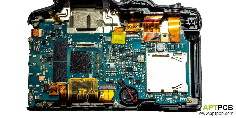
Image Sensor Interface Design and Signal Integrity
Modern CMOS image sensors output data through LVDS, sub-LVDS, or MIPI CSI-2 interfaces at rates that can exceed 10 Gbps aggregate for high-resolution sensors operating at high frame rates. A 50MP sensor capturing 14-bit RAW data at 20fps generates approximately 17.5 Gbps of raw data—requiring careful PCB implementation to maintain signal integrity across the sensor-to-processor interface.
The sensor interface typically uses flexible PCB connections between sensor module and main board, allowing sensor positioning independent of main board location. This flex section must maintain impedance control for high-speed differential pairs while providing mechanical compliance for focus and stabilization mechanisms.
Sensor Interface Implementation
- Interface Protocol: MIPI CSI-2 dominant in compact cameras; LVDS/sub-LVDS in larger sensors; SLVS-EC emerging for highest-bandwidth applications exceeding 4 Gbps/lane.
- Differential Pair Routing: 100Ω differential impedance for MIPI; tight length matching within pairs (<5 mil skew); adequate pair-to-pair spacing (≥2× trace width).
- Flex Interface: Controlled-impedance flex from sensor module; flex thickness and construction affects achievable impedance—design flex section explicitly for interface requirements.
- Reference Plane Continuity: Uninterrupted ground reference beneath sensor interface traces; via stitching along routing maintains return path integrity.
- Termination Design: On-die termination typical; external termination rarely needed but design should allow option if signal integrity issues arise during development.
- Connector Selection: Fine-pitch board-to-flex connectors with controlled impedance; connector bandwidth must exceed interface requirements with margin.
Sensor interface quality directly affects achievable image quality—noise coupling, reflection, and jitter all degrade sensor output before processing begins.
Image Processor Implementation and Memory Requirements
Camera image processors handle computationally-intensive tasks: demosaicing, noise reduction, color processing, compression, and increasingly computational photography features. These processors require high-bandwidth memory interfaces for image buffering—continuous shooting modes may capture dozens of full-resolution images per second, requiring sustained memory bandwidth exceeding 10 GB/s.
To keep fine-pitch BGAs routable and shorten DDR escape routing, many camera boards use HDI PCB technology (microvias, via-in-pad, and tighter trace/space).
The combination of high-speed memory interfaces and substantial processor power dissipation (5-15W for advanced processors) creates demanding PCB requirements. Memory routing must maintain signal integrity at DDR4/LPDDR4 speeds while power delivery and thermal design support sustained high-performance operation.
Processor and Memory Design
- Memory Architecture: LPDDR4/4X dominant for power efficiency; DDR4 for maximum bandwidth—interface speed selection based on burst capture depth and video requirements.
- Memory Routing: Standard DDR guidelines apply—length matching within byte lanes, DQS-to-DQ matching, and consistent impedance; camera applications typically use x32 or x64 interfaces.
- Processor Fanout: BGA packages with 0.5-0.65mm pitch require HDI or careful via-in-pad planning; layer count driven by memory interface complexity.
- Decoupling Strategy: Extensive decoupling for processor power rails; ceramic capacitors distributed around package periphery plus bulk capacitance nearby.
- Clock Distribution: Image pipeline clocks require low jitter; dedicated oscillators or PLL outputs with clean power supplies and isolated routing.
- Card Interface: SD/CFexpress card interfaces for image storage; controlled-impedance routing for high-speed UHS-II/III SD or CFexpress NVMe interfaces.
High-bandwidth memory interfaces benefit from high-speed PCB design principles ensuring adequate timing margins across temperature and production variation.
Precision Analog Design for Image Quality
Image quality depends on analog performance throughout the signal chain—sensor power supply noise directly couples into images as pattern noise, analog gain stages add their own noise contribution, and ADC reference quality affects quantization accuracy. Premium cameras achieve 14-15 stops of dynamic range, requiring noise floors below 2 electrons RMS—demands that propagate through the entire analog design.
The mixed-signal nature of camera PCBs creates challenges: high-speed digital processors and memory generate substantial noise that must be prevented from coupling into sensitive analog circuits. Effective partition and isolation strategies are essential.
Analog Design Considerations
- Sensor Power Supplies: Ultra-low-noise LDOs (<10μVRMS) for sensor analog supplies; PSRR >60dB at 100kHz prevents supply ripple from appearing in images.
- Ground Partitioning: Separate analog and digital ground regions; single-point connection prevents digital return currents from flowing through analog circuits.
- Analog Routing Isolation: Sensor analog outputs (if any external analog) require shielded routing; guard traces connected to analog ground.
- Reference Generation: ADC references require stable, low-noise generation; dedicated reference ICs or filtered internal references based on performance requirements.
- Thermal Stability: Analog component drift with temperature affects calibration; consider temperature coefficients in component selection.
- EMI Immunity: External electromagnetic interference can couple into analog circuits; appropriate shielding and filtering at enclosure entry points.
Analog performance in cameras directly correlates with image quality—noise floor improvements enable higher usable ISO settings and better shadow detail.
Thermal Management in Camera Bodies
Camera thermal design affects both continuous operation capability (video recording, burst shooting) and user experience (uncomfortable grip temperature). Image processors dissipating 5-15W in compact bodies generate significant heat that must transfer through the enclosure without exceeding component limits or user comfort thresholds.
The sensor itself requires thermal management—sensor temperature affects noise performance (each 6-8°C increase roughly doubles dark current), and sustained video recording or live view can elevate sensor temperatures significantly. Some cameras implement active cooling for video-centric use cases.
Thermal Design Strategies
- Heat Spreading: Copper planes beneath processors spread heat across larger area; internal ground planes serve dual electrical and thermal functions.
- Thermal Via Arrays: Dense via arrays conduct heat from top-layer components to inner layers and bottom surface; filled vias provide better thermal conductivity.
- Heat Sink Interface: Metal frame contact areas provide thermal path to camera body; flat copper pours with thermal interface material bridge PCB-to-frame gap.
- Processor Throttling: Design thermal solution for sustained operation without throttling; verify continuous video recording duration meets specifications.
- Sensor Thermal Isolation: Consider thermal isolation between sensor and hot processor areas; flex connection provides some thermal resistance.
- Component Placement: Spread heat-generating components across board; avoid concentrating processor, power supplies, and wireless modules in one area.
Thermal performance determines continuous operation capability—critical for video-focused cameras requiring extended recording times.
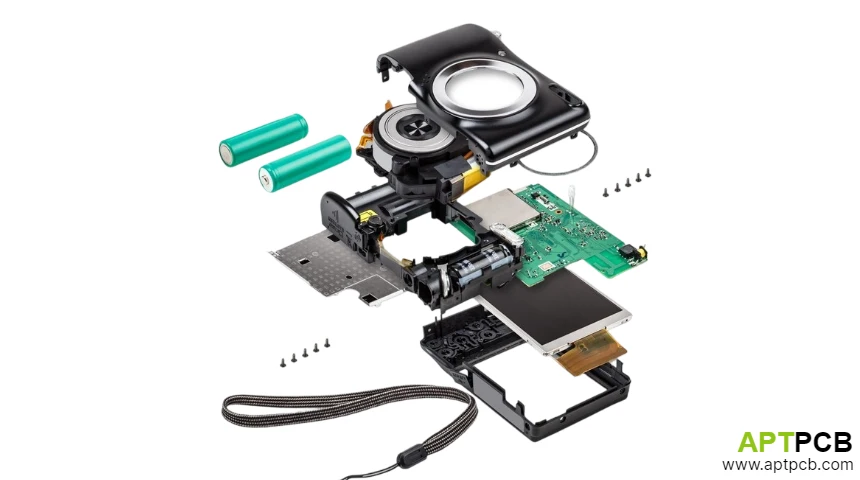
Flex-Rigid Construction for Camera Systems
Camera systems extensively use flex-rigid construction to connect multiple PCBs within compact bodies while allowing independent positioning for optical alignment. Typical implementations include main board to sensor module, main board to rear display, and main board to top control interface—each connection potentially using flex circuits rather than discrete cables.
The flex sections must accommodate assembly sequences, service access requirements, and in some cases ongoing mechanical motion (articulating displays, lens movement during focus/zoom). These requirements drive flex material selection, layer count, and bend radius design.
Flex-Rigid Implementation
- Sensor Module Connection: Controlled-impedance flex for high-speed sensor interface; polyimide construction for thermal stability during soldering.
- Display Interface: MIPI DSI or LVDS to rear LCD; flex routing through hinge for articulating displays requires dynamic flex rating.
- Control Interfaces: Button, dial, and touch interfaces through flex; typically lower-speed signals with relaxed routing requirements.
- Bend Radius Management: Static bends (assembled once) permit tighter radius than dynamic (repeated motion); design flex length to achieve required radius without strain.
- Stiffener Application: Stiffeners on flex at connector and component mounting locations; polyimide or FR-4 stiffeners depending on thickness and rigidity requirements.
- Assembly Sequence: Flex-rigid assemblies require specific assembly order; design for manufacturable assembly sequence with appropriate test access.
Using rigid-flex PCB construction can eliminate bulky board-to-board cabling, making tight camera mechanical stacks more reliable and easier to assemble.
Manufacturing Requirements for Imaging Electronics
Camera PCB manufacturing requires attention to both precision assembly (fine-pitch BGAs, HDI structures) and analog performance (consistent impedance, clean power planes). The mixed-signal nature demands quality controls beyond typical digital assembly—electrical characteristics affecting image quality must be verified.
Production testing for cameras includes functional verification of all interfaces, calibration of image processing parameters, and potentially image quality assessment using test targets. The test strategy must balance throughput requirements against quality verification depth.
Manufacturing Considerations
- HDI Fabrication: Sensor and processor fanout often requires HDI; consistent microvia quality and registration essential for yield.
- Impedance Control: Sensor interface impedance tolerance affects high-speed signal integrity; TDR verification on production samples.
- Flex-Rigid Quality: Flex-rigid junction reliability critical; cross-section inspection verifies construction integrity.
- Cleanliness Control: Imaging electronics sensitive to contamination; ionic contamination testing and cleanliness protocols during assembly.
- Functional Calibration: Camera calibration during production affects out-of-box image quality; automated calibration systems with test targets.
- ESD Protection: Image sensors extremely ESD-sensitive; strict ESD controls throughout assembly and handling.
For imaging products, consistent process control in multilayer PCB fabrication matters as much as fine-pitch assembly—stackup accuracy, via quality, and cleanliness directly influence signal integrity and noise.
Technical Summary
Digital camera PCB design combines high-speed digital expertise for sensor and memory interfaces with precision analog design for image quality. The mixed-signal challenges require careful partitioning, power supply design, and layout discipline that prevents digital noise from degrading analog performance.
Key decisions include sensor interface implementation (protocol selection, flex design), memory architecture (bandwidth versus power trade-offs), thermal strategy (sustained operation capability), and flex-rigid architecture (connectivity approach within mechanical constraints).
Manufacturing partnerships should evaluate both high-speed digital capabilities (HDI, fine-pitch assembly) and analog process control (cleanliness, ESD handling) appropriate for imaging electronics requirements.
If you’re building an imaging product and need a board stackup that balances bandwidth, noise, and manufacturability, explore our full range of PCB capabilities.