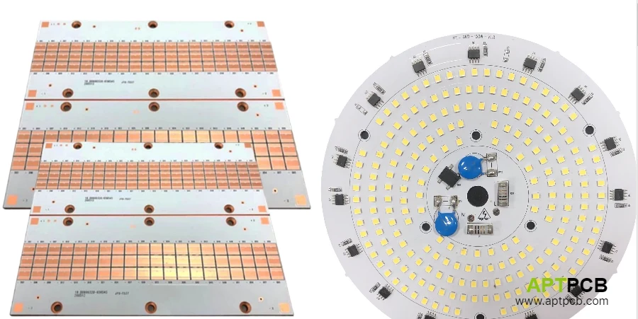
High power LED applications—automotive headlamps, stadium lighting, industrial fixtures, and professional stage illumination—push thermal management to extremes that standard LED PCB approaches cannot address. Power densities exceeding 10 W/cm² create junction temperatures that rapidly degrade LED performance unless thermal design receives engineering attention proportional to the challenge.
The thermal path from LED junction to ambient determines whether high power LEDs achieve rated output and lifetime or fail prematurely through accelerated lumen depreciation and color shift. Each element in this path—die attach, LED package, solder joint, PCB substrate, thermal interface material, and heatsink—contributes thermal resistance that accumulates toward junction temperature.
This guide addresses high power LED PCB design for applications where thermal performance determines product viability.
Analyzing High Power LED Thermal Requirements
High power LED thermal analysis quantifies the challenge before solution development begins. Power dissipation, acceptable junction temperature, available thermal paths, and environmental conditions establish requirements that substrate selection and thermal design must meet.
Consider a 50W LED array in an enclosed industrial fixture with 45°C ambient: at 50% optical efficiency, 25W dissipates as heat. Maintaining 85°C junction temperature leaves only 40°C thermal budget for the entire path from junction to ambient. Allocating this budget across multiple thermal resistances—and meeting each allocation—requires systematic analysis.
Thermal Analysis Framework
- Power Dissipation Calculation: Total heat = Electrical power × (1 - optical efficiency). High power LEDs typically achieve 40-60% efficiency; use conservative efficiency estimate for thermal design.
- Junction Temperature Target: Select based on lifetime and performance requirements. Premium applications target 75-85°C junction for maximum lifetime; cost-sensitive products may accept 95-105°C with reduced lifetime.
- Thermal Budget Allocation: Distribute available temperature rise across path elements: LED package (fixed by LED selection), solder interface (0.1-0.3°C/W achievable), substrate (design variable), TIM (0.1-0.5°C/W), heatsink (application dependent).
- Environmental Boundary Conditions: Maximum ambient temperature, available heatsink area, natural vs forced convection, solar loading for outdoor applications. Design for worst-case combined conditions.
- Spreading Resistance Consideration: For concentrated heat sources, spreading resistance can dominate total thermal resistance. High thermal conductivity substrates reduce spreading resistance but may still require design attention for extreme concentrations.
- Transient Thermal Analysis: Some applications involve pulsed operation where thermal mass provides buffering. Analyze both steady-state and transient conditions to determine limiting case.
Selecting Advanced Thermal Substrates
Substrate selection for high power LEDs requires matching thermal capability to power density requirements while balancing cost, manufacturability, and application constraints. The technology spectrum from enhanced MCPCB through ceramic substrates provides options across the performance-cost continuum.
Standard aluminum MCPCB with 1.0 W/m·K dielectric serves many commercial LED applications but may prove inadequate for true high-power designs. Enhanced dielectric formulations, copper-core construction, and ceramic substrates each address limitations of standard materials—at progressively higher cost.
Substrate Technology Options
- Enhanced Aluminum MCPCB (2.0-3.0 W/m·K): Upgraded dielectric formulations reduce thermal resistance to 0.33-0.5°C·cm²/W versus 1.0°C·cm²/W for standard material. Cost premium of 1.5-2× often justified for demanding applications. Maintains standard MCPCB fabrication compatibility.
- Copper Core MCPCB: Copper's thermal conductivity (385 W/m·K vs aluminum's 150 W/m·K) provides superior spreading for concentrated heat sources. Weight and cost increase (2.5-3.5× aluminum) limit use to applications where spreading resistance dominates thermal budget.
- Direct Thermal Path Substrates: Architectures eliminating polymer dielectric entirely—direct copper bonding to ceramic or specialized metal-ceramic hybrids. Maximum thermal performance for applications where cost permits.
- Alumina Ceramic (Al₂O₃): Direct thermal path without polymer bottleneck. Thermal conductivity 24-28 W/m·K, achieving thermal resistance of 0.02-0.04°C·cm²/W. Ceramic PCB technology suits power modules and high-reliability applications.
- Aluminum Nitride (AlN): Premium ceramic with 170-200 W/m·K conductivity—approaching copper while maintaining electrical isolation. Cost of 5-10× MCPCB limits use to extreme applications where alternatives prove inadequate.
- Thermal Substrate Selection Criteria: Match capability to requirement without over-specification. Enhanced MCPCB serves most high-power applications; ceramic justified only when analysis demonstrates MCPCB inadequacy.
Optimizing Heat Spreading Design
Heat spreading distributes concentrated power from LED sources across larger substrate area before extraction to heatsink. Effective spreading reduces peak temperatures and improves heatsink utilization. Spreading design interacts with substrate selection—higher conductivity substrates spread more effectively but spreading geometry also matters.
Spreading Design Principles
- Spreading Angle Estimation: Heat spreads at approximately 45° angle in homogeneous materials. For thin substrates relative to heat source size, this angle significantly affects spreading effectiveness.
- Copper Weight Impact: Heavier copper layers improve lateral spreading before heat enters substrate through-thickness. Heavy copper construction (3-6oz) can reduce peak temperatures 5-15°C versus standard 1oz copper.
- Copper Pour Design: Extend copper pours well beyond LED footprint—ideally to board edges or mounting holes enabling heatsink contact. Avoid thermal relief patterns under LED pads that impede heat flow.
- Thermal Via Enhancement: For FR-4 or hybrid constructions, dense thermal via arrays (0.3mm diameter, 0.6mm pitch) under heat sources provide parallel thermal paths. Via filling and capping prevents solder wicking issues.
- Internal Layer Utilization: Multilayer constructions can use internal copper layers for spreading, though through-layer thermal resistance still limits effectiveness. Consider this approach for applications combining routing complexity with thermal requirements.
- Simulation Validation: Complex spreading geometries benefit from thermal simulation during design. Verify spreading effectiveness and identify hot spots before prototyping commitment.
Engineering Solder Joint Thermal Interface
The solder joint between LED package and PCB represents a critical thermal interface often overlooked in high power design. Voids within the solder joint reduce effective contact area, creating thermal bottleneck that can undermine carefully designed substrate thermal performance.
Thermal pad void content directly affects thermal resistance. Voids covering 25% of pad area can increase thermal resistance 30-50% depending on void distribution. For high power applications where thermal margins are tight, void control becomes essential rather than optional.
Solder Joint Optimization
- Thermal Pad Size: Size thermal pads to match or exceed LED package thermal slug dimensions. Extending copper 1-2mm beyond package provides additional spreading area without affecting solder joint formation.
- Solder Paste Stencil Design: Subdivide large thermal pad apertures into grid patterns preventing void-trapping. Target 50-70% coverage with individual apertures below 1.5mm × 1.5mm. Balance paste volume against void risk.
- Reflow Profile Optimization: Extend soak times allowing volatile release before reflow. Profile development using thermocouples on actual LED packages ensures adequate reflow without exceeding LED thermal limits.
- Void Specification and Verification: Specify maximum acceptable void percentage (typically 15-25% for high-power applications) and implement X-ray inspection for verification. Sample or 100% inspection based on application criticality.
- Solder Alloy Selection: Standard SAC305 suits most applications. Consider alloys with improved thermal conductivity or void characteristics for demanding applications.
- Process Control: Void formation has multiple root causes—paste chemistry, stencil design, profile parameters, substrate cleanliness. Establish process controls addressing each contributor.
Designing Thermal Interface to Heatsink
The interface between PCB substrate and heatsink significantly affects system thermal performance. Thermal interface materials (TIMs) bridge surface imperfections, but introduce their own thermal resistance requiring optimization within system thermal budget.
Thermal Interface Design
- Interface Material Selection: Match TIM type to application: thermal grease for reworkable assemblies, phase-change materials for improved long-term performance, thermal pads for gap filling and assembly ease. Each presents thermal resistance and practical trade-offs.
- Contact Area Maximization: Design PCB with maximum flat area contacting heatsink. Avoid cutouts, standoffs, and features reducing contact area unless functionally necessary. Appropriate board profiling maintains flatness.
- Mounting Pressure Specification: TIM thermal resistance depends on applied pressure. Specify mounting torque and hardware ensuring adequate, consistent pressure across contact area without substrate damage.
- TIM Thermal Resistance Accounting: TIM contributes 0.1-0.5°C/W depending on material, thickness, and pressure. Include actual TIM specification in thermal budget—manufacturer claims often assume ideal conditions.
- Assembly Process Definition: Document TIM application method ensuring consistent coverage without voids or excessive squeeze-out. Include in assembly process documentation.
- Long-term Stability: Some TIMs degrade through pump-out during thermal cycling or dry-out at elevated temperature. Select materials with demonstrated stability for application lifetime and conditions.
Ensuring High Power LED Reliability
High power LED reliability depends on maintaining junction temperature within acceptable limits throughout product life—not just at initial operation. Thermal design margin, aging effects, and environmental variations all affect long-term reliability that determines warranty exposure and customer satisfaction.
Reliability Engineering Considerations
- Design Margin Implementation: Build 10-15°C margin between calculated junction temperature and maximum rating to accommodate manufacturing variation, component aging, and environmental uncertainty.
- Thermal Cycling Analysis: Repeated temperature excursions stress solder joints and interfaces. High-Tg materials improve thermal cycling survival; verify interface stability through cycling qualification testing.
- Lifetime Prediction: LED manufacturer lifetime data enables reliability prediction based on junction temperature. Select LED operating point achieving reliability targets with margin.
- Failure Mode Consideration: Common high power LED failure modes include solder joint cracking, wire bond fatigue, phosphor degradation, and driver failure. Design addressing each mode's root cause.
- Qualification Testing: Establish qualification protocol including thermal cycling, high-temperature operating life, humidity exposure, and any application-specific stresses. Comprehensive test protocols validate design robustness.
- Production Monitoring: Implement ongoing production monitoring (void inspection, forward voltage distribution, light output sampling) detecting drift before it creates field failures.
Summary
High power LED PCB design centers on thermal management at every level: substrate selection providing fundamental thermal capability, spreading design distributing heat from concentrated sources, solder joint optimization maintaining thermal interface integrity, and system integration ensuring effective heat extraction to ambient.
The investment in proper thermal design pays dividends through reliable field performance. High power LED products with inadequate thermal design may function initially but fail prematurely—creating warranty costs, reputation damage, and customer dissatisfaction far exceeding the cost of proper thermal engineering during development.
Success requires systematic analysis establishing requirements, informed substrate selection matching capability to requirements, and disciplined implementation ensuring thermal design intent survives manufacturing variation.