
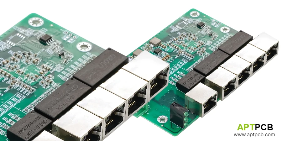
An industrial gateway PCB is not only a controller board. It is a boundary assembly that connects different electrical worlds: field wiring, industrial communication ports, power conversion, embedded processing, and external networks.
A successful review must answer four questions before fabrication:
- Where does the field environment end and the protected electronics domain begin?
- Which interfaces require physical isolation, protection, or controlled return paths?
- Can manufacturing clearly build and inspect the released design?
- Can the assembled gateway be powered, programmed, and tested without redesigning the fixture during production?
For application positioning, start with industrial control PCB. If processor density, power conversion, or enclosure restrictions create thermal challenges, keep high-thermal PCB as a design path. If the main concern is production verification after assembly, include FCT test during the early design review.
Quick Answer
An industrial gateway PCB should be released as a managed interface assembly. The connector map, isolation boundaries, power domains, mechanical constraints, and production test access should be reviewed together. A gateway that passes schematic review can still fail manufacturing if isolation gaps, probe access, connector variants, or bring-up procedures remain undefined.
Table of Contents
- 1. What Makes Industrial Gateway PCB Review Different
- 2. How Should Interface Zones Be Partitioned
- 3. How Do Isolation Boundaries Affect PCB Manufacturing
- 4. Industrial Gateway PCB Review Decision Matrix
- 5. What Should Be Included in the Manufacturing Handoff Package
- 6. How Should Functional Testing Be Planned
- Conclusion: Treat the Gateway PCB as an Interface Contract
1. What Makes Industrial Gateway PCB Review Different
Industrial gateway boards usually combine several functional regions:
- field connectors for industrial equipment
- protection circuits for external wiring
- isolated communication interfaces
- processor and memory circuits
- Ethernet, wireless, or cloud-facing communication modules
- DC input and power conversion sections
- service and programming interfaces
The challenge is not simply fitting components into a PCB outline. The challenge is maintaining clear ownership between electrical domains.
A gateway may connect a noisy OT environment containing long cables, switching equipment, and field transients with a sensitive processor running application software. The PCB must physically support that separation.
The main manufacturing risks usually appear when design intent is not converted into measurable release information:
- an isolation boundary exists only in the schematic
- connector variants are not frozen before assembly
- shield or enclosure requirements are missing
- test access is considered after routing is complete
- production limits are confused with engineering validation requirements
2. How Should Interface Zones Be Partitioned?
A gateway PCB layout becomes easier to manufacture when zones follow system boundaries rather than component categories.
Recommended functional zones include:
| PCB Zone | Typical Contents | Main Review Focus |
|---|---|---|
| Field Interface Zone | terminal blocks, RS-485, CAN, protection devices | surge path, connector strength, isolation |
| Power Entry Zone | DC input, filters, regulators, protection | heat, current path, switching noise |
| Processing Zone | MCU, SoC, memory, clocks | signal integrity, thermal margin |
| Communication Zone | Ethernet PHY, wireless modules, antennas | grounding, impedance, placement |
| Service Zone | programming headers, debug connectors, test points | accessibility, fixture compatibility |
Keeping these areas visually and electrically separated improves DFM review because fabrication, assembly, and test teams can evaluate the same design intent.
For example, Ethernet interfaces may require magnetics placement and controlled routing considerations, while fieldbus interfaces may require isolation and surge protection planning. These should not be treated as identical interface blocks.
3. How Do Isolation Boundaries Affect PCB Manufacturing?
Isolation is not only a component selection decision. It is a physical PCB structure.
A schematic may include digital isolators, transformers, or optocouplers, but the PCB must preserve the intended separation through:
- creepage distance
- clearance spacing
- isolation slots
- copper keep-outs
- connector placement
- shield and chassis-ground strategy
A typical industrial gateway may separate a field side using 24 V or 48 V industrial connections from a processor domain containing sensitive digital electronics.
The review should confirm:
- whether the isolation boundary is visible in fabrication drawings
- whether copper pours cross the intended separation area
- whether vias unintentionally bridge isolated regions
- whether connectors create reduced spacing at board edges
- whether contamination-sensitive areas have enough physical margin
Isolation Boundary Risk Table
| Design Area | Possible Issue | Manufacturing Impact |
|---|---|---|
| Isolation slot | Slot position unclear | Fabrication interpretation risk |
| Connector edge | Reduced creepage distance | Assembly and reliability concern |
| Copper plane | Crosses isolation region | Electrical failure risk |
| Shield connection | Undefined return path | EMC troubleshooting delay |
| Test point placement | Located across boundary | Fixture limitation |
If processor heat or power density becomes a board-level issue, route the thermal discussion to high-thermal PCB. The correct solution depends on whether heat must leave through the PCB structure or through the enclosure.
4. Industrial Gateway PCB Review Decision Matrix
A practical release review can use the following decision matrix:
| Design Question | Low Complexity Gateway | Industrial Production Gateway | High-Reliability Gateway |
|---|---|---|---|
| Interface count | Few fixed ports | Multiple field interfaces | Multiple isolated domains |
| Test approach | Manual verification | Fixture-based FCT | Automated production test |
| Isolation review | Basic spacing check | Defined boundary documentation | Formal isolation validation |
| Thermal planning | Standard FR-4 review | Copper and airflow analysis | Dedicated thermal strategy |
| Manufacturing package | Gerber + BOM | Full build package | Controlled release process |
The correct manufacturing path depends on the final operating environment, production volume, and validation requirements.
5. What Should Be Included in the Manufacturing Handoff Package?
Before RFQ or pilot build, provide a release package that connects engineering intent with production execution.
A complete package should include:
- Gerber or ODB++ fabrication data
- PCB stack-up requirements
- BOM with approved alternatives
- connector and mechanical drawings
- isolation boundary definition
- keep-out requirements
- programming method
- test-point map
- expected powered test sequence
- enclosure constraints
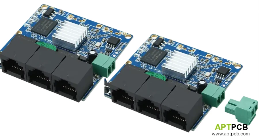
Connector strategy deserves early attention because industrial gateway boards often contain:
- terminal blocks
- shielded Ethernet connectors
- module sockets
- service headers
- mounting interfaces
Mechanical changes late in the process frequently affect assembly yield and test access.
6. How Should Functional Testing Be Planned?
Gateway products are validated at the PCBA level, not only at the bare-board level.
The test handoff should define which checks belong to each manufacturing stage.
| Test Stage | Typical Purpose |
|---|---|
| Bare PCB inspection | Verify fabrication quality |
| SMT inspection | Confirm assembly placement |
| AOI/X-ray | Check solder and hidden joints |
| Programming | Load controlled firmware image |
| Functional test | Verify powered operation and interfaces |
A gateway functional test plan may include:
- power-up behavior
- communication-port presence
- connector mapping verification
- firmware loading confirmation
- Ethernet or field-interface response
- basic input/output checks
The path into FCT test should be considered during PCB design. Test points, service headers, and fixture access become expensive changes after assembly tooling begins.
Conclusion: Treat the Gateway PCB as an Interface Contract
Industrial gateway PCB projects become easier to manufacture when the board is treated as a contract between electrical design, mechanical design, assembly, and test teams.
The most important release decisions are:
- define interface boundaries early
- document isolation physically
- separate power, field, and processor domains
- freeze connector and enclosure assumptions
- plan production test before layout completion
For industrial applications, begin with industrial control PCB, then consider high-thermal PCB or FCT test depending on the main production risk.
Related pages & tools
Use this route when the gateway belongs to a cabinet, PLC-adjacent, DIN-rail, or industrial automation system.
Use this route when powered verification, interface testing, and fixture planning determine production readiness.
Use this route when processor or power-stage heat requires board-level thermal planning.
Move here after the interface map, stack-up, BOM, and test expectations are prepared.
Next steps: Request an Isolation Boundary & DFM Review
If your industrial gateway design contains multiple field interfaces, uncertain isolation boundaries, or incomplete production-test planning, send the release package through quote.
Include:
- Gerber or ODB++
- stack-up information
- BOM
- connector map
- isolation requirements
- test expectations
APTPCB engineering review can help identify manufacturing risks before prototype production, including isolation definition issues, assembly constraints, and functional-test access limitations.
Public references
Analog Devices, "MT-031: Grounding Data Converters and Solving the Mystery of AGND and DGND"
IPC-2581 Consortium, "What is IPC-2581?"
Keysight, "Functional Test Systems for Electronics Manufacturing"
Cisco, "Industrial Networking Design Guides"
Author and review information
- Author: APTPCB industrial connectivity content team
- Technical review: PCB manufacturing, PCBA process, industrial-control layout, and functional-test engineering team
- Last updated: 2025-01-11
Ensure harsh environment durability by specifying PCB conformal coating on field-deployed gateways.