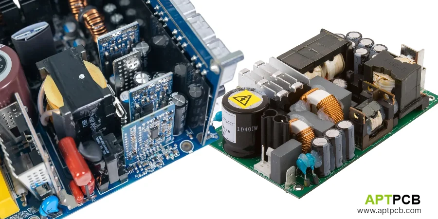
Industrial power supplies convert AC mains or DC bus power to regulated voltages that automation equipment requires. The PCB must achieve high efficiency while meeting safety isolation requirements, providing hold-up time for controlled shutdown during power interruptions, and surviving voltage transients and harmonics that industrial electrical systems generate.
This guide covers PCB design decisions that determine industrial power supply reliability, efficiency, and regulatory compliance.
In This Guide
- Wide Input Range Design
- Transformer and Isolation Design
- Output Regulation and Load Sharing
- Hold-Up Time and Energy Storage
- Thermal Management in Enclosed Spaces
- EMC and Safety Compliance
Wide Input Range Design
Industrial power supplies operate from diverse power sources—85-264VAC universal input for global deployment, 380-480VAC three-phase for high-power applications, or 18-75VDC for DC-powered systems. The PCB design must accommodate the component stresses and control range that wide input operation imposes.
Universal AC input requires power factor correction (PFC) at power levels above 75W to meet IEC 61000-3-2 harmonic limits. The PFC stage boosts input voltage to a regulated DC bus (typically 380-400VDC), enabling consistent operation across the input range while controlling harmonic current draw. Active PFC achieves >0.95 power factor and <10% THD.
Component stress varies dramatically across input voltage range. At minimum input voltage, primary current maximizes and conduction losses peak. At maximum input voltage, voltage stress on semiconductors and capacitors reaches maximum. The heavy copper PCB construction must handle both conditions reliably.
Wide Input Design Considerations
- PFC Topology: Continuous conduction mode boost for medium power; bridgeless or interleaved for high efficiency at higher power.
- Inrush Limiting: NTC thermistor or active limiting prevents tripping upstream breakers at turn-on.
- Input Capacitor Sizing: Bulk capacitors sized for maximum ripple current at minimum input voltage.
- Voltage Sensing: Accurate input voltage sensing enables control optimization and fault detection.
- Transient Rating: Design survives input transients per IEC 61000-4-5 without damage.
- Three-Phase Considerations: Phase loss detection and operation for three-phase input systems.
Transformer and Isolation Design
Safety isolation between AC mains and output circuits requires transformer construction and PCB layout that meet creepage, clearance, and dielectric withstand requirements of safety standards. The transformer core, winding arrangement, and PCB placement determine both safety compliance and leakage inductance that affects efficiency.
Transformer leakage inductance stores energy that must dissipate during switching, contributing to switching losses and EMI. PCB traces connecting transformer windings to semiconductors add inductance that appears in the switching loop. Minimizing this inductance through careful layout improves efficiency and reduces voltage spikes.
The PCB stackup and layout around the transformer must maintain safety spacing. Creepage and clearance requirements depend on working voltage, pollution degree, and insulation type (basic, supplementary, reinforced). Slots or cutouts in the PCB may be needed to achieve required creepage distances in compact designs.
Isolation Design Requirements
- Creepage/Clearance: Per IEC 60664-1 for working voltage and pollution degree; reinforced insulation typically requires 5.5-8mm.
- Transformer Construction: Triple-insulated wire or bobbin construction that maintains isolation under fault conditions.
- PCB Slots: Routed slots under transformer increase creepage where solid material spacing is insufficient.
- Ground Plane Splits: Primary and secondary ground planes separated by isolation barrier with no unintended coupling.
- Y Capacitor Selection: Safety-rated capacitors across isolation barrier for EMI filtering without compromising safety.
- Optocoupler/Transformer Feedback: Isolated feedback maintains regulation accuracy while preserving isolation integrity.
Output Regulation and Load Sharing
Industrial power supplies must maintain output voltage within ±1-2% under varying load conditions, including transient response during load steps and regulation across distributed wiring to multiple loads. Multiple output designs require consideration of cross-regulation and load sharing.
Output voltage sensing should occur at the load connection point, not at the power supply terminals, to compensate for wiring resistance. Remote sense connections allow the control loop to regulate at the actual load despite voltage drop in distribution wiring. However, remote sense adds complexity and potential noise pickup that the PCB design must address.
Parallel operation for higher power or redundancy requires load sharing mechanisms. Droop sharing varies output voltage slightly with load current, while active current sharing uses dedicated control signals between paralleled units. The industrial control PCB design must support these features while maintaining transient response.
Output Regulation Design
- Output LC Filtering: LC filter provides low output ripple while maintaining transient response.
- Remote Sense: Differential sense inputs with ESD protection and filtering for noise immunity.
- Minimum Load: Design operates stable across full output range including light load or no load.
- Multiple Outputs: Cross-regulation specification for multi-output designs; post-regulators if cross-regulation is critical.
- Parallel Operation: Current sharing accuracy ±5-10% between paralleled units.
- Transient Response: Voltage deviation and recovery time specified for standard load step (e.g., 50% load change).
Hold-Up Time and Energy Storage
Industrial systems require continued operation during brief power interruptions that occur during switching events or short brownouts. Hold-up time—the duration the power supply maintains regulated output after input power loss—allows systems to complete operations or execute controlled shutdown.
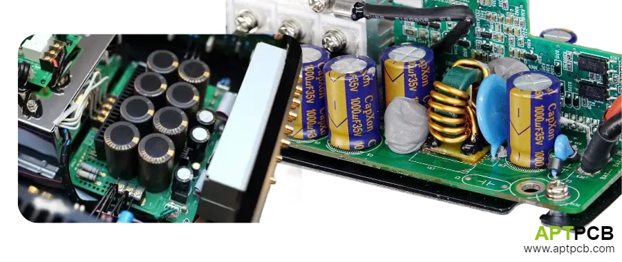
Typical industrial requirements specify 20-50ms hold-up time at full load. The energy storage comes primarily from bulk capacitors in the DC link (post-PFC bus) and output stage. Capacitor sizing must account for the energy required to maintain output voltage for the specified duration at rated load.
Longer hold-up times require larger capacitors, increasing cost and size. Alternatively, external UPS or capacitor banks provide extended holdup for critical systems. The PCB must provide mounting and connections for bulk capacitors while managing ripple current heating that affects capacitor life. Power electronics PCB design must balance these competing requirements.
Hold-Up Energy Storage
- Capacitor Sizing: Energy stored must exceed load energy demand during hold-up period with margin.
- Ripple Current Rating: Capacitor ripple current rating must exceed worst-case switching ripple without excessive heating.
- ESR Consideration: Low-ESR capacitors reduce self-heating and improve transient response.
- Capacitor Lifetime: Electrolytic capacitor life depends on temperature and ripple current; design targets exceed 10-year life.
- Power Good Signal: Output monitor indicates when output voltage falls below specification during power loss.
- Controlled Shutdown: Hold-up time allows systems to save state and complete controlled shutdown.
Thermal Management in Enclosed Spaces
Industrial power supplies mount in electrical enclosures with limited airflow, elevated ambient temperatures, and heat contribution from adjacent equipment. The PCB thermal design must dissipate power losses to enclosure surfaces without exceeding component temperature limits.
Efficiency directly affects thermal requirements—a 100W supply with 90% efficiency dissipates 11W internally, while 95% efficiency reduces dissipation to 5.3W. Higher efficiency justifies added component cost through reduced heatsink requirements, improved reliability, and lower cooling burden on enclosures.
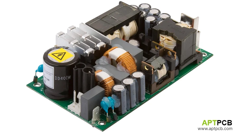
Component placement on thermal management PCBs distributes heat generation across available cooling surfaces. Power semiconductors, inductors, and transformers—the primary heat sources—position for effective heat transfer to enclosure surfaces or internal heatsinks. Electrolytic capacitors locate away from hot spots to maximize lifetime.
Thermal Design Approaches
- Efficiency Targets: 90%+ efficiency for standard products; 95%+ for high-density or enclosed applications.
- Derating Curves: Published output current versus ambient temperature derating for design guidance.
- Component Placement: Heat-generating components near cooling surfaces; sensitive components in cooler zones.
- Airflow Independence: Design for natural convection operation; forced air cooling optional for higher power.
- Thermal Via Arrays: Copper vias conduct heat from surface-mount power devices to internal or bottom copper planes.
- Enclosure Coordination: Thermal design coordinates with enclosure manufacturer for heat path optimization.
EMC and Safety Compliance
Industrial power supplies must meet EMC requirements (IEC 61000-6-2 immunity, IEC 61000-6-4 emissions) and safety standards (IEC 62368-1 or IEC 60950-1). Compliance requires coordinated design of filtering, shielding, grounding, and isolation from concept through production.
EMC filtering at the input attenuates conducted emissions from switching converters. Common-mode chokes with X and Y capacitors form multi-stage filters that achieve 40-60dB attenuation in the 150kHz-30MHz conducted emissions band. Filter effectiveness depends on component selection, PCB layout, and parasitic coupling paths that bypass intended attenuation.
Safety compliance requires documentation of isolation distances, temperature rise under fault conditions, and dielectric withstand testing results. The PCB manufacturing process must maintain these critical dimensions—creepage distances eroded by poor edge definition or solder bridges compromise safety compliance.
Compliance Design Requirements
- Conducted Emissions: Input filter achieves Class A or Class B limits across operating range.
- Radiated Emissions: PCB layout and shielding control radiation from switching nodes and cables.
- Surge Immunity: Survives 1kV line-to-line, 2kV line-to-ground surges per IEC 61000-4-5.
- Safety Certification: UL/CSA, CE marking, and regional certifications as required for target markets.
- Temperature Testing: Component temperatures documented under maximum load and ambient conditions.
- Production Testing: Hi-pot testing verifies isolation integrity for every unit produced.
Summary
Industrial power supply PCB design combines power electronics with safety and regulatory requirements in systems that must operate reliably for decades in challenging environments. Wide input range operation, efficiency optimization, hold-up time capability, and compliance with EMC and safety standards create competing constraints that require careful engineering trade-offs. The resulting designs enable the automation systems that depend on reliable, efficient power conversion.