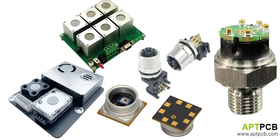
Industrial sensors measure temperature, pressure, flow, level, and position in process environments where electrical noise, temperature extremes, and physical hazards challenge measurement accuracy and electronics reliability. The PCB must extract millivolt signals from sensing elements while rejecting interference that may exceed the desired signal by orders of magnitude.
This guide covers PCB design approaches that achieve precision measurement in industrial conditions.
In This Guide
- Sensor Signal Conditioning
- Noise Rejection and EMI Immunity
- Loop-Powered Circuit Design
- Communication Interface Implementation
- Environmental Protection
- Intrinsic Safety Considerations
Sensor Signal Conditioning
Industrial sensors produce various signal types requiring specialized conditioning: RTD and thermocouple temperature sensors generate millivolt signals needing amplification; strain gauge bridges produce microvolt-level outputs; piezoelectric sensors source charge rather than voltage. The PCB front-end must match the sensing element characteristics while achieving required accuracy.
Thermocouple conditioning requires cold junction compensation and linearization across the sensor's temperature range. The reference junction temperature measurement accuracy directly affects overall accuracy—1°C reference error creates 40µV measurement error for Type K thermocouples, equivalent to ~1°C process error.
RTD conditioning uses constant current excitation with ratiometric measurement that cancels excitation drift. Three-wire and four-wire configurations eliminate lead resistance effects that would otherwise introduce temperature-dependent errors. The multilayer PCB stackup must maintain measurement accuracy across the operating temperature range.
Signal Conditioning Design
- Instrumentation Amplifiers: High CMRR (>80dB) rejection of common-mode interference on sensor leads.
- Excitation Stability: Current source stability and noise affect measurement accuracy in resistance-based sensors.
- ADC Resolution: 16-24 bit ADCs provide resolution exceeding sensor accuracy for digital processing margin.
- Anti-Alias Filtering: Appropriate filter bandwidth prevents aliased noise from corrupting measurements.
- Reference Accuracy: Voltage reference stability contributes directly to measurement accuracy.
- Calibration Architecture: Hardware supports multi-point calibration for sensor linearization.
Noise Rejection and EMI Immunity
Industrial environments generate electromagnetic interference from motor drives, welding equipment, switching contactors, and radio transmitters that can corrupt sensor measurements. The PCB must reject this interference while maintaining measurement bandwidth for process dynamics.
Common-mode rejection eliminates interference that appears equally on both sensor leads—typically from electromagnetic coupling to sensor wiring. Instrumentation amplifier CMRR performance at interference frequencies determines rejection effectiveness; CMRR falls with frequency, making high-frequency interference harder to reject.
Differential-mode interference appears between sensor leads and cannot be rejected by common-mode techniques. Filtering must attenuate this interference while passing the measurement signal. For slowly-varying process measurements, aggressive low-pass filtering (0.1-10Hz bandwidth) significantly improves noise rejection. high-frequency PCB design techniques ensure the sensor PCB operates reliably in industrial EMI environments.
Noise Rejection Techniques
- Input Filtering: RC or active filters at sensor inputs reject high-frequency interference before amplification.
- Shielded Routing: Sensor signal traces routed with guard traces or dedicated shielded layers.
- Ground Plane Integrity: Unbroken ground planes under analog sections provide low-impedance return paths.
- Isolation: Galvanic isolation between sensor input and communication output breaks ground loops.
- Averaging and Oversampling: Digital averaging improves effective resolution and rejects non-correlated noise.
- Synchronous Detection: For AC-excited sensors, synchronous detection extracts signal from interference.
Loop-Powered Circuit Design
4-20mA loop-powered transmitters derive operating power from the measurement current loop, eliminating the need for local power supplies. This architecture has powered industrial sensors for decades but constrains the PCB design to operate within strict power budgets—typically 3.5-4mA during measurement.
The PCB must include all signal conditioning, processing, and communication functions within the loop power budget. Microcontrollers enter low-power sleep modes between measurements; analog front-ends use auto-ranging to minimize power; communication occurs in bursts during available power windows.
Loop voltage compliance range (minimum to maximum loop voltage across which the transmitter operates correctly) depends on the power management design. Low-power industrial electronics must maintain accuracy across this voltage range while surviving transients and reverse polarity events.
Loop-Powered Design
- Power Budget: Total power consumption ≤3.5mA × (Vloop_min - Vdrop) throughout operation.
- Startup Sequence: Controlled power-up sequence as loop current establishes operating voltage.
- Voltage Regulation: Low-dropout regulators or switching converters extract maximum power from limited budget.
- Sleep Modes: Processor and analog sections enter low-power states between measurement cycles.
- HART Communication: Power during HART FSK modulation peaks constrained by loop power.
- Reverse Polarity Protection: Protection against installation errors without excessive forward voltage drop.
Communication Interface Implementation
Industrial sensors communicate via 4-20mA current loops with HART overlay, fieldbus protocols (PROFIBUS PA, Foundation Fieldbus), or industrial Ethernet. Each interface presents distinct PCB design requirements for isolation, signal integrity, and power management.
HART (Highway Addressable Remote Transducer) overlays FSK-modulated digital communication on the 4-20mA current loop. The PCB must modulate and demodulate HART signals without disturbing the analog current signal—filtering separates the 1200/2200 Hz HART carrier from the DC current measurement.
Fieldbus protocols require isolated communication transceivers and bus power derivation in field-powered architectures. high-speed PCB routing must maintain isolation integrity while achieving required data rates and distances.
Communication Implementation
- 4-20mA Output: Precision current DAC with compliance voltage range and protection circuits.
- HART Modem: FSK modem IC with appropriate filtering for carrier separation.
- Fieldbus Interface: Protocol-specific transceiver with isolation and bus power management.
- Industrial Ethernet: Isolated Ethernet interface for IO-Link or Ethernet-based sensor protocols.
- Wireless Options: Bluetooth LE or WirelessHART for battery-powered wireless sensors.
- Configuration Interface: Local interface (HART, USB, or display) for sensor configuration.
Environmental Protection
Industrial sensors operate in environments with temperature extremes, humidity, vibration, and corrosive atmospheres that destroy unprotected electronics. The PCB design and construction must survive these conditions while maintaining measurement accuracy.
Temperature range requirements vary by application—process sensors may require -40°C to +85°C operation, while sensors mounted near hot processes need even wider ranges. Component selection must account for parameter drift with temperature; calibration may include temperature compensation coefficients.
Conformal coating protects against humidity and contamination but affects thermal paths and may trap moisture if applied over wet boards. Potting provides maximum protection but complicates rework and may stress components through thermal expansion mismatch. The substrate and construction choices—including ceramic PCB options for high-temperature or chemically aggressive environments—must support the selected protection methods.
Environmental Protection Approaches
- Conformal Coating: Acrylic or silicone coating for humidity protection; selective coating avoids connectors and thermal interfaces.
- Potting: Epoxy or silicone potting for maximum protection in harsh environments.
- Material Selection: High-Tg PCB materials for elevated temperature operation.
- Component Selection: Industrial or automotive-grade components rated for required temperature range.
- Moisture Barrier: Hermetic sealing for sensors in condensing or washdown environments.
- Vibration Resistance: Staking of heavy components; strain relief on connections.
Intrinsic Safety Considerations
Sensors installed in hazardous locations with explosive atmospheres require intrinsically safe (IS) or explosion-proof construction. Intrinsically safe designs limit energy available for ignition through circuit design constraints that affect PCB layout, component selection, and spacing.
IS barriers limit voltage, current, and stored energy to levels below ignition thresholds for specific gas groups. The PCB layout must maintain creepage and clearance distances that prevent breakdown under fault conditions. Infallible components (resistors, diodes with current limiting) provide fault tolerance that enables IS certification.
Entity parameters (Vmax, Imax, Ci, Li) specify the maximum voltage, current, capacitance, and inductance that the sensor presents to IS barriers. PCB design must document and control these parameters for certification. Industrial safety design practices ensure the sensor meets hazardous location requirements.
Intrinsic Safety Design
- Barrier Interface: Design for connection to IS barriers with specified entity parameters.
- Energy Limiting: Current-limiting resistors and zener diodes limit fault energy.
- Spacing Requirements: Creepage and clearance per IEC 60079-11 for working voltage and pollution degree.
- Component Certification: Use of certified IS components where available; evaluation of standard components otherwise.
- Capacitance Control: PCB and cable capacitance documented and controlled within entity limits.
- Inductance Control: Wiring and component inductance documented and controlled.
Summary
Industrial sensor PCB design blends precision analog measurement with rugged reliability for harsh environments—noise, temperature extremes, surge events, vibration, and (sometimes) hazardous-location requirements.
Strong designs start with the front-end: the right signal conditioning for RTDs/thermocouples/bridges, aggressive input filtering, and layout/partitioning that protects microvolt–millivolt signals from EMI. For loop-powered 4–20mA transmitters, power budgeting and low-drop protection/regulation are just as critical as accuracy. Finally, isolation, creepage/clearance, conformal coating or potting choices, and intrinsic-safety documentation help ensure the design stays accurate and dependable over long service life.
If you’re building industrial sensing hardware, see our full PCB manufacturing.