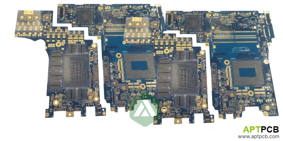
Laptop motherboards concentrate desktop-class computing power into boards measuring roughly 250mm × 200mm—often smaller for ultrabooks. This compression demands careful attention to high-speed signal integrity for DDR5 memory interfaces, robust power delivery for processors drawing 45-65W (gaming laptops exceed 150W combined CPU+GPU), thermal management within chassis constraints, and manufacturing quality that ensures reliability through years of thermal cycling and mechanical stress.
This guide addresses the PCB-specific challenges in laptop design: layer stackup optimization for signal integrity and power delivery, DDR5 and PCIe routing constraints, power delivery network design for modern processors, thermal strategies that work within notebook form factors, and the manufacturing capabilities necessary for consistent production quality.
In This Guide
- Layer Stackup Design for High-Speed and Power Integrity
- DDR5 Memory Interface Routing Requirements
- CPU and GPU Power Delivery Network Design
- Thermal Management Through PCB Design
- Manufacturing Considerations for Laptop Motherboards
- Reliability Testing and Quality Requirements
Layer Stackup Design for High-Speed and Power Integrity
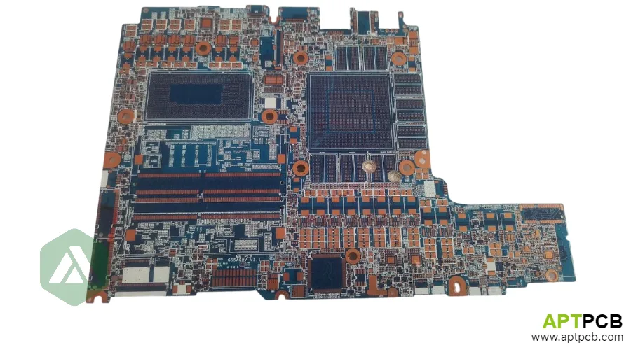
Laptop motherboards typically employ 8-12 layer constructions, balancing signal routing capacity against thickness and cost constraints. The stackup must accommodate DDR5 interfaces operating at 4800-6400 MT/s, PCIe Gen4/Gen5 lanes at 16-32 GT/s, USB4/Thunderbolt at 40-80 Gbps, and substantial power distribution for high-TDP processors—all within 1.0-1.6mm total thickness.
A typical 10-layer laptop motherboard stackup dedicates two layers to ground reference planes, two layers to power distribution (split among multiple voltage rails), and six layers to signal routing. The arrangement places high-speed signals on layers immediately adjacent to uninterrupted ground planes, providing controlled impedance and return current paths essential for signal integrity at multi-gigabit rates.
Stackup Architecture Considerations
- Ground Plane Continuity: DDR5 and PCIe signals require uninterrupted ground reference; avoid routing through ground plane areas beneath high-speed signals—via anti-pads and splits create return path discontinuities that degrade signal quality.
- Power Plane Segmentation: Modern laptops require numerous voltage rails (VCORE, VGT for GPU, VDDQ for memory, multiple I/O voltages); power planes segment into isolated regions with careful attention to current return paths.
- Dielectric Selection: Standard FR-4 (Dk ~4.2-4.4) suffices for DDR5 at current speeds; PCIe Gen5 and USB4 benefit from mid-loss materials (Dk ~3.5-3.8, Df <0.008) for long traces.
- Copper Weights: Inner power layers use 1oz or 2oz copper for adequate current capacity; signal layers typically 0.5oz or 1oz depending on current requirements and trace width constraints.
- Impedance Targets: DDR5 data/DQS typically 40Ω single-ended; PCIe/USB4 differential pairs 85-100Ω; careful prepreg thickness control maintains ±10% impedance tolerance.
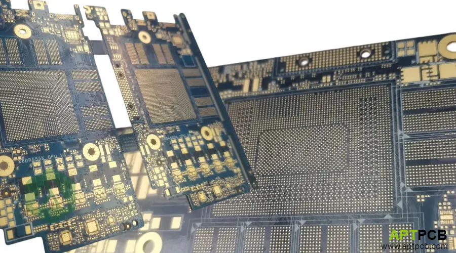
- Via Structures: Through-hole vias for power delivery; blind/buried vias (HDI) increasingly common for BGA fanout density requirements on CPU and PCH packages.
Working with manufacturers experienced in multilayer PCB fabrication ensures stackup designs are manufacturable with consistent impedance control across production volumes.
DDR5 Memory Interface Routing Requirements
DDR5 memory interfaces present significant PCB routing challenges—data rates up to 6400 MT/s (and beyond for future JEDEC specifications) push signal integrity requirements to levels previously associated with high-frequency RF design. The DDR5 architecture change from single-channel to dual-channel per DIMM means each memory slot requires routing twice the signal count of DDR4, though at reduced loading.
Length matching requirements remain stringent: data bits within a byte lane (DQ0-7) must match within ±2mm; DQS strobe to data within ±5mm; command/address to clock within ±25mm. At 6400 MT/s, these tolerances correspond to timing margins that leave no room for manufacturing variation or temperature effects—proper design technique is essential.
DDR5 Routing Guidelines
- Topology Changes: DDR5 eliminates the multi-drop topology of earlier generations; point-to-point from CPU to each DIMM channel simplifies routing but still requires careful length matching and impedance control.
- On-Die Termination: DDR5 moves termination on-die, eliminating board-level termination resistors for data signals; reduces component count but requires attention to stub lengths at DIMM connectors.
- Power Delivery: DDR5 integrates voltage regulation on the DIMM (PMIC); motherboard provides 5V input to DIMM rather than 1.1V VDDQ—changes power plane requirements versus DDR4.
- Differential Clock Routing: DDR5 uses differential clocking; 85Ω differential impedance with tight coupling and length matching within ±1mm.
- Via Optimization: Memory signal vias should minimize stub length; back-drilling available but adds cost; design via placement to minimize layer transitions.
- Crosstalk Management: Maintain 3× line width spacing between memory signals; ground fills between differential pairs help isolation.
Achieving consistent DDR5 performance requires high-speed PCB design expertise and manufacturing processes capable of maintaining tight impedance tolerances across production.
CPU and GPU Power Delivery Network Design
Modern laptop processors demand power delivery systems rivaling desktop implementations—a 65W laptop CPU might draw 150A at 0.8V during transient loads, while gaming laptops with discrete GPUs can exceed 300A total between CPU and GPU power rails. The PCB power delivery network (PDN) must provide stable voltage with minimal droop under load transients, requiring careful plane design, decoupling strategy, and VRM placement.
The PDN impedance target derives from transient current requirements and acceptable voltage variation. A target impedance of 5mΩ flat to 100MHz keeps voltage variation within 2% for typical Intel/AMD processor specifications. Achieving this impedance requires bulk capacitors (hundreds of μF), mid-frequency ceramics (10-100μF), and high-frequency ceramics (100nF-10μF) distributed appropriately on the board.
Power Delivery Design Strategies
- Plane Copper Weight: Power planes serving CPU/GPU require 2oz copper minimum; 3oz for high-TDP designs—current density should not exceed 35A/mm² for acceptable temperature rise.
- Plane Shape Optimization: VCORE plane should extend beneath processor package with minimal via penetrations; simulate current distribution to identify bottlenecks.
- Decoupling Capacitor Placement: Bulk capacitors (470μF+) near VRM; mid-frequency ceramics distributed along power plane edges; high-frequency ceramics directly at processor pins (underneath if using blind vias).
- VRM Component Placement: Place power stage inductors and MOSFETs as close to processor as thermal constraints allow; longer power delivery paths increase parasitic inductance and transient response time.
- Current Sensing: Many designs include current sense resistors in power path; placement affects accuracy—locate at VRM output before distribution splits.
- Via Current Capacity: Power delivery vias conduct significant current; use via arrays rather than single vias—each 0.3mm via safely carries ~1A DC; thermal analysis verifies via temperature.
Understanding heavy copper PCB requirements helps ensure power delivery designs are manufacturable and meet current-carrying requirements without excessive temperature rise.
Thermal Management Through PCB Design
Laptop thermal solutions rely on heat pipes and fans to remove heat from processor packages, but the PCB plays a crucial secondary role in heat spreading and provides the thermal interface between components and cooling systems. PCB thermal design affects both processor performance (inadequate cooling causes throttling) and long-term reliability (thermal cycling stress causes solder joint fatigue).
The PCB beneath processor packages serves as an initial heat spreader—thermal vias conduct heat from the top-layer BGA connection to internal copper planes and the bottom surface. For components without direct heat sink contact (chipset, voltage regulators, memory), the PCB may be the primary thermal path, making copper plane coverage critical.
PCB Thermal Design Approaches
- Thermal Via Arrays: Dense via arrays (0.3mm drill, 0.5mm pitch) beneath processor and GPU packages conduct heat vertically; filled vias prevent solder wicking and improve thermal continuity.
- Copper Plane Utilization: Maximize copper coverage on inner layers beneath thermal-critical components; 2oz copper on thermal layers if stackup permits.
- Component Thermal Pads: VRMs, chipsets, and other medium-power components often use thermal pads to chassis ground planes; PCB must provide adequate copper area at connection points.
- Heat Sink Mounting: Laptop heat sinks mount via spring clips or screws; PCB mounting holes must provide electrical isolation (if not grounded) and mechanical support without cracking.
- Thermal Expansion Management: Large processor packages (45mm+) experience differential expansion versus PCB; adequate underfill and proper solder joint design prevent crack propagation.
- Temperature Monitoring: Thermal sensor placement (thermistors or thermal diodes in processor packages) provides feedback for fan control; ensure sensors have good thermal coupling to monitored components.
Integration of PCB thermal design with system cooling solutions requires understanding both thermal management principles and mechanical interface requirements.
Manufacturing Considerations for Laptop Motherboards
Laptop motherboard manufacturing combines moderate HDI complexity (blind/buried vias for BGA fanout) with high volume production requirements and quality expectations approaching automotive standards. Major OEMs—Dell, HP, Lenovo, Apple—impose supplier qualification requirements including process capability studies, statistical process control, and ongoing reliability monitoring.
The fine-pitch BGA packages used for CPU and PCH (0.4-0.8mm pitch) demand precise drilling registration, controlled copper plating, and consistent solder mask application. Manufacturing variation directly impacts assembly yield—poorly controlled via registration or solder mask alignment causes assembly defects that only appear after expensive component placement.
Manufacturing Requirements
- HDI Capability: Many laptop designs require blind vias (1+N+1 or 2+N+2 structures) for adequate BGA fanout; via-in-pad with filled and capped construction for maximum routing density.
- Drill Registration: Blind via registration to underlying layers within ±50μm; layer-to-layer alignment across all layers within ±75μm.
- Solder Mask Quality: LPI solder mask with controlled dam width between fine-pitch pads; registration to features within ±50μm.
- Surface Finish: ENIG preferred for fine-pitch BGA reliability; controlled thickness (3-5μin Au, 100-200μin Ni) prevents both excessive and insufficient gold.
- Impedance Control: DDR5 and PCIe traces require ±8% impedance tolerance; demonstrated through TDR measurement on production coupons.
- Panel Utilization: Board size and panel optimization affect cost; irregular laptop shapes may limit panel utilization below 70%—design consideration during early development.
Selecting manufacturing partners with demonstrated PCB fabrication capabilities for HDI structures and fine-pitch applications ensures designs translate to manufacturable production.
Reliability Testing and Quality Requirements
Laptop computers face demanding reliability expectations—consumers expect 5+ years of useful life with daily use patterns that include thermal cycling (sleep-wake cycles cause repeated temperature transitions), mechanical stress (opening/closing, carrying in bags), and environmental exposure (humidity, dust). PCB quality and reliability directly affect warranty costs and brand reputation.
Major OEMs specify extensive qualification testing beyond standard IPC acceptance criteria. Typical requirements include accelerated thermal cycling (1000+ cycles, -40°C to +105°C), humidity exposure (85°C/85%RH for 1000 hours), mechanical shock and vibration, and powered thermal cycling that simulates actual use conditions.
Quality and Reliability Framework
- IPC Class 2/3: Most laptop PCBs specify IPC-6012 Class 2 minimum; premium products and business-class laptops may require Class 3 for tighter tolerances and enhanced reliability.
- Microsection Inspection: Cross-section analysis verifies copper plating quality, via structure integrity, and dielectric thickness; performed on qualification lots and ongoing production sampling.
- Electrical Testing: 100% continuity and isolation testing via flying probe or fixture; controlled impedance verification on high-speed traces.
- Thermal Cycling: Qualification includes extensive thermal cycling; failure criteria include via resistance increase, laminate delamination, and solder mask cracking.
- CAF Resistance: Conductive anodic filament (CAF) testing verifies resistance to electrochemical migration between closely-spaced conductors; critical for fine-pitch designs.
- Traceability: Full lot traceability from laminate materials through finished boards; essential for failure analysis correlation and continuous improvement.
Robust quality management systems with documented procedures, calibrated equipment, and trained personnel form the foundation for consistent laptop PCB quality.
Technical Summary
Laptop motherboard PCB design balances competing requirements: high-speed signal integrity for DDR5 and PCIe interfaces, robust power delivery for high-TDP processors, thermal management within constrained form factors, and manufacturing quality that ensures long-term reliability. Success requires integrated design considering all aspects simultaneously rather than optimizing each in isolation.
Key decisions early in laptop development include layer count and stackup architecture (determining signal integrity and power delivery capability), HDI complexity level (affecting cost and manufacturing complexity), thermal strategy (PCB's role in overall cooling solution), and quality/reliability targets (driving material selection and manufacturing requirements).
The PCB manufacturing partner relationship proves critical—laptop programs involve significant volume production with aggressive cost targets, yet quality requirements approach automotive levels. Manufacturing capability, process maturity, and quality systems all factor into partner selection alongside cost considerations.