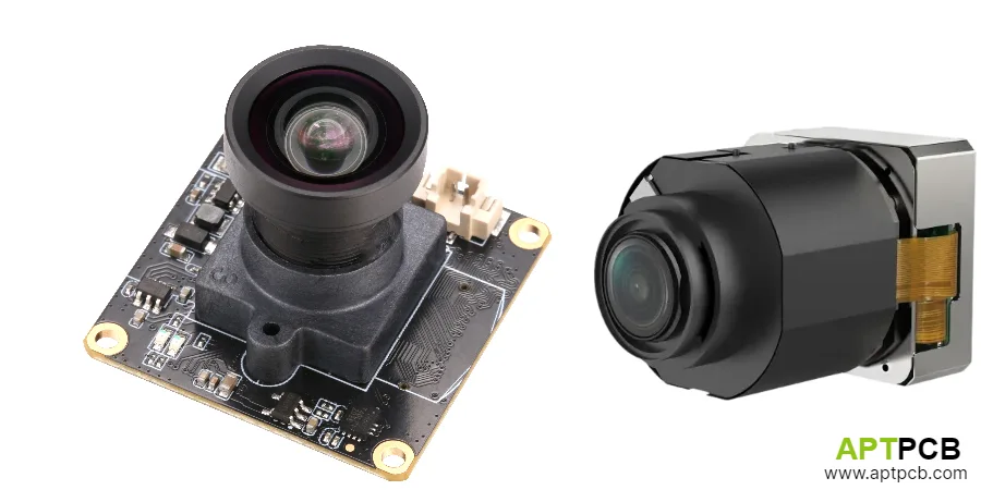
Machine vision cameras capture images for automated inspection, guidance, and measurement at frame rates from a few Hz to thousands of frames per second. The PCB must interface to image sensors, process and transfer gigabytes per second of image data, and respond to external triggers with microsecond-level precision—all within the thermal and mechanical constraints of compact camera housings.
This guide covers PCB design considerations that determine machine vision camera performance and reliability in industrial environments.
In This Guide
- Image Sensor Interface Design
- High-Speed Data Path Architecture
- Trigger and Synchronization
- Power Management for Sensors
- Thermal Management in Compact Housings
- Industrial Interface Implementation
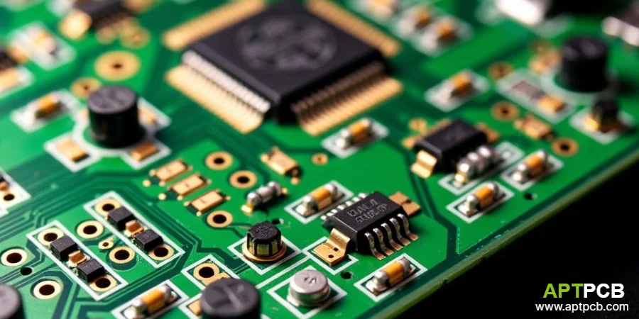
Image Sensor Interface Design
CMOS image sensors output data through parallel LVDS interfaces, MIPI CSI-2, or Sub-LVDS protocols at data rates reaching multi-gigabits per second. The PCB interface must maintain signal integrity from sensor to FPGA or processor through controlled impedance routing with tight length matching.
LVDS sensor interfaces use multiple differential pairs carrying clock and data at rates from 200Mbps to 1Gbps per lane. Skew between data lanes and clock affects data capture reliability—typical requirements specify lane-to-lane skew within 0.1UI (unit interval), translating to a few millimeters of trace length matching for high-speed interfaces.
MIPI CSI-2 interfaces provide standardized high-bandwidth connections but require careful attention to impedance control and termination. High-speed PCB design techniques for these interfaces include controlled impedance routing, proper via transitions, and attention to return path continuity.
Sensor Interface Requirements
- Impedance Control: 100Ω differential for LVDS; 85-100Ω differential for MIPI CSI-2 depending on specification version.
- Length Matching: Intra-pair matching within 2 mils; lane-to-lane matching per sensor timing requirements.
- Reference Planes: Unbroken reference planes under high-speed traces; controlled via transitions.
- Termination: On-die termination common in sensors; external termination if required by interface specification.
- Power Filtering: Separate analog and digital sensor supplies with appropriate filtering.
- Sensor Mounting: Controlled sensor-to-board alignment for optical precision.
High-Speed Data Path Architecture
Image data flows from sensor through FPGA processing to output interface at sustained rates of several gigabits per second. A 5-megapixel sensor at 100fps with 10-bit depth generates 5Gbps continuous data. The PCB data paths must sustain this bandwidth without creating thermal or signal integrity problems.
FPGA selection balances I/O bandwidth, processing resources, and power consumption. High-speed serial transceivers (5-10 Gbps per channel) handle Camera Link, CoaXPress, or 10GigE outputs. The multilayer PCB stackup must support multiple high-speed interfaces while managing crosstalk and maintaining impedance control.
Memory interfaces for frame buffers add additional high-speed routing. DDR3/DDR4 interfaces require careful attention to timing, while newer HyperRAM or LPDDR4x options offer simpler routing at adequate bandwidth for many applications.
Data Path Design
- FPGA I/O Planning: Group related interfaces on the same FPGA bank; plan power supplies by bank requirements.
- Memory Interface: DDR timing constraints drive PCB layer assignment and routing rules.
- High-Speed Routing: Microstrip for top-layer routing; stripline for inner layers with controlled coupling.
- Via Transitions: Back-drilled or blind/buried vias minimize stubs for multi-gigabit signals.
- Power Integrity: PDN design supports transient current demands from FPGA and memory.
- Crosstalk Budget: Spacing and shielding maintain crosstalk below interface noise margins.
Trigger and Synchronization
Machine vision applications often require precise timing between image capture and external events—strobe lights, part position, or motion controller commands. The camera must respond to trigger inputs with known, minimal latency and may need to synchronize multiple cameras for stereo or multi-view imaging.
Trigger input circuits must reject electrical noise common in factory environments while achieving fast response. Optocoupler isolation protects camera electronics but adds propagation delay; high-speed digital isolators offer faster response when isolation is required. Input filtering must pass legitimate trigger edges while rejecting noise.
Frame synchronization between multiple cameras uses hardware trigger distribution or IEEE 1588/PTP. To keep clocks clean and escapes short around fine‑pitch PHYs and connectors, many designs benefit from HDI PCB fabrication.
Trigger System Design
- Input Characteristics: 5-24V input range typical for industrial compatibility; configurable edge polarity.
- Debouncing: Hardware or firmware debouncing rejects contact bounce without excessive delay.
- Latency Specification: Documented trigger-to-exposure latency with jitter specification.
- Isolation Options: Optocoupler or digital isolator for ground loop protection.
- Strobe Output: Synchronized strobe trigger output with programmable timing offset.
- Multi-Camera Sync: Hardware trigger distribution or PTP timestamp correlation.
Power Management for Sensors
Image sensor power supplies directly affect image quality. Noise on analog supplies appears as fixed pattern noise in captured images; supply ripple at certain frequencies creates visible banding artifacts. The PCB power distribution must provide clean, stable supplies to achieve sensor performance specifications.
Large image sensors consume 1-3W, creating localized heating that affects dark current and noise performance. Power sequencing requirements from sensor manufacturers must be followed precisely—incorrect sequencing can damage sensors or cause latch-up. The power electronics design must meet both quality and sequencing requirements.
Power-over-Ethernet (PoE) cameras derive operating power from the Ethernet connection, eliminating separate power wiring. The PCB must include PoE PD (powered device) circuitry with isolated DC-DC conversion to meet sensor supply requirements.
Power Design for Image Sensors
- Supply Noise: Analog supplies require <10mVpp ripple; tighter specs for scientific cameras.
- LDO vs. Switching: LDOs provide lower noise; switching acceptable with adequate filtering.
- Sequencing: Power sequencing per sensor datasheet; monitor-based sequencing for complex requirements.
- Bulk Capacitance: Adequate capacitance for transient current during sensor readout.
- Thermal Coordination: Power dissipation location affects sensor thermal environment.
- PoE Integration: IEEE 802.3af/at PD interface with isolated DC-DC for PoE cameras.
Thermal Management in Compact Housings
Machine vision cameras package electronics with significant power dissipation—10-25W typical for industrial cameras—into compact housings that may lack ventilation. The PCB thermal design must conduct heat to housing surfaces for dissipation while maintaining sensor temperature within operating limits.
Image sensor temperature affects noise performance. Dark current doubles approximately every 6-8°C, increasing noise floor at elevated temperatures. Critical applications may require active cooling (TEC) to maintain consistent sensor temperature; the PCB must support TEC power delivery and temperature monitoring.
The thermal PCB design must balance heat spreading requirements with high-speed signal integrity. Heavy copper planes improve thermal conductivity but may affect controlled impedance; careful stackup design achieves both thermal and electrical requirements.
Thermal Design Approaches
- Heat Spreading: Copper planes conduct heat from localized sources to housing contact areas.
- Thermal Interface: Thermal pads or gap fillers transfer heat from PCB to housing.
- Component Placement: Hot components positioned for effective heat paths; sensitive circuits in cooler zones.
- Sensor Thermal Path: Dedicated thermal path from sensor to housing, possibly through metal carrier.
- TEC Support: TEC drive circuitry and temperature monitoring for cooled sensors.
- Airflow Consideration: For cameras with ventilation, component placement considers airflow patterns.
Industrial Interface Implementation
Machine vision cameras connect to host systems via GigE Vision, Camera Link, CoaXPress, or USB3 Vision interfaces. Each interface has distinct PCB requirements for signal integrity, connector selection, and power delivery.
GigE Vision cameras use standard Ethernet PHY with industrial-grade magnetics and connectors. Screw-lock M12 or RJ45 with cable retention handle vibration and cable stress. The PHY and transformer layout follows high-speed PCB manufacturing for signal integrity and EMC.
CoaXPress cameras transmit high-bandwidth video over coaxial cable with power delivery on the same cable. The PCB interface includes high-speed serializer, coax driver, and PoCXP power extraction circuitry.
Interface Implementation
- GigE Vision: Industrial Ethernet PHY; M12 or locking RJ45 connectors; 1500Vrms isolation.
- Camera Link: Parallel LVDS interface; MDR26 or SDR26 connectors; cable equalization for long cables.
- CoaXPress: High-speed SERDES; coax connector and driver; power extraction for PoCXP.
- USB3 Vision: USB 3.0 controller; screw-lock USB connectors for industrial retention.
- GPIO Interface: Isolated digital I/O for trigger input and strobe output.
- Configuration Interface: Serial interface for camera configuration and firmware update.
Summary
Machine vision camera PCB design integrates high-speed sensor interfaces, gigabit data paths, precision timing, and thermal management into compact packages that must operate reliably in industrial environments. The combination of signal integrity challenges, power quality requirements, and thermal constraints in limited volumes creates design complexities that require coordinated engineering across multiple domains. Success depends on understanding how image quality requirements translate into PCB design specifications and manufacturing tolerances.