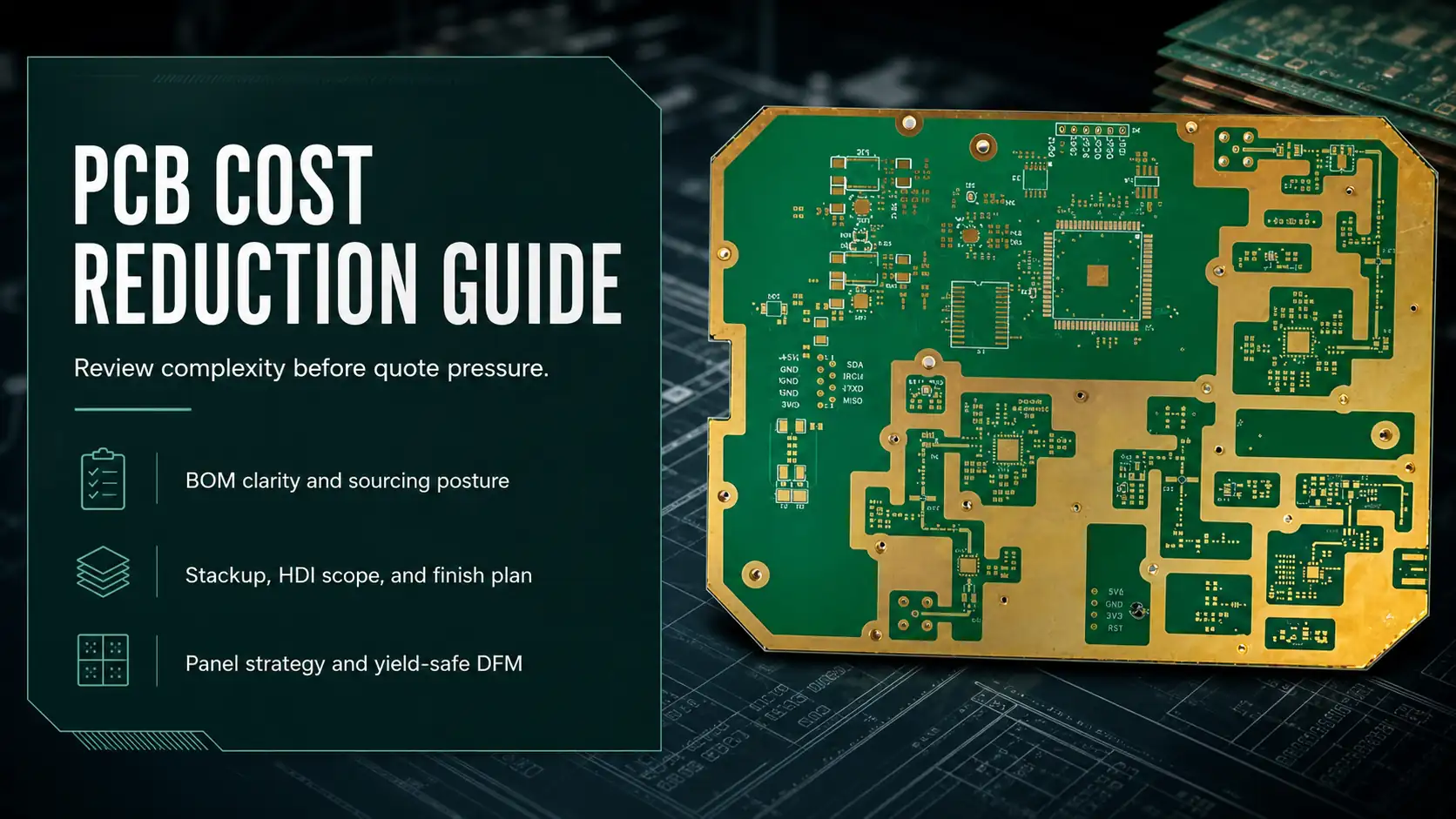
- PCB cost reduction works best when it is treated as an engineering review problem, not as a generic promise that every board can be made cheaper.
- The real cost drivers usually appear where the board moves from a baseline multilayer route into a more complex process family: stackup changes, HDI features, finish requirements, tooling, and validation scope.
- The safest way to reduce avoidable cost is to remove unnecessary complexity and freeze the RFQ package before DFM and quote review begin.
- A useful guide should combine pricing logic, manufacturability logic, and yield-safe simplification instead of separating them into four partially overlapping blog posts.
Quick Answer
If you want to reduce PCB cost without creating new manufacturing risk, start by reviewing the project in this order: BOM clarity, stackup intent, board-family route, HDI or special-process scope, finish plan, panel strategy, and validation expectations. The goal is not to force every board into the cheapest possible recipe. The goal is to remove avoidable complexity before the board reaches DFM and quote review.
Table of Contents
- What does PCB cost reduction actually mean?
- Where does PCB cost usually come from?
- Which inputs usually move the quote first?
- How do stackup and board family change cost?
- When do HDI and special processes raise quote complexity?
- How do surface finish, testing, and tooling affect price?
- Which DFM changes can reduce cost without adding yield risk?
- What changes when you move from prototype to volume?
- What should be frozen before RFQ?
- Next steps with APTPCB
- FAQ
- Public references
- Author and review information
What does PCB cost reduction actually mean?
Here, PCB cost reduction means reducing avoidable quote complexity, process escalation, and manufacturability friction before production release.
That framing matters because many cost-themed articles make two mistakes:
- they treat material cost as if it were the whole story
- they present yield, lead time, or savings as guaranteed outcomes
Neither is a safe public framing for real PCB programs.
The better question is:
Which design or package decisions are increasing fabrication and assembly complexity beyond what the product actually needs?
That question pulls four related cost discussions into one practical review:
- cost reduction
- cost drivers
- price breakdown
- yield-safe simplification
When those topics are handled in one place, the reader gets a more realistic workflow:
- understand what affects quote posture
- identify which choices increase complexity
- simplify what is not required
- freeze the package before RFQ
Where does PCB cost usually come from?
PCB cost rarely comes from one isolated variable. In most projects, quote complexity is easier to review when it is separated into four layers.
| Cost layer | What belongs here | Why it matters |
|---|---|---|
| Material system | Laminate family, copper weight, prepreg choices, finish family | Material and finish choices can move the board into a different process lane |
| Fabrication route | Layer count, lamination route, drill strategy, HDI scope, controlled structures | Process steps increase when the structure becomes more specialized |
| Testing and validation | Flying probe, fixtures, coupons, inspection scope, release evidence | Validation expectations can expand the quote package even when artwork stays the same |
| Engineering and setup | CAM review, panel planning, tooling, process clarification | Cleanup before RFQ often reduces re-quote cycles and late engineering loops |
This is the public-safe way to discuss material vs. process vs. testing without pretending there is one universal cost formula for every PCB.
How to read a PCB cost breakdown chart
A PCB cost breakdown chart can still be useful, but it should be treated as an illustrative engineering diagram, not as a fixed public pricing promise.
One useful way to frame the chart is:
Material SystemFabrication RouteTesting and ValidationEngineering and Setup
For example:
Illustrative view of the main cost buckets that influence PCB quote complexity. Actual project weighting varies by stackup, process family, validation scope, and order volume.
That keeps the visual useful without turning it into an unsupported pricing commitment.
Illustrative view of the four review layers that usually shape PCB quote complexity: material system, fabrication route, testing and validation, and engineering/setup.
Which inputs usually move the quote first?
The first quote changes usually come from package definition, not from one isolated trace rule.
| Review area | What to check | Why it changes quote posture |
|---|---|---|
| BOM clarity | Part identity, alternates, sourcing posture, assembly scope | Ambiguous BOM data creates delay before fabrication review is even stable |
| Stackup definition | Layer count, impedance intent, material family, lamination assumptions | The build path changes when the board stops being a baseline multilayer job |
| Board-family route | Baseline multilayer, HDI, hybrid RF, heavy copper, or another special-process family | Similar-looking boards can require very different factory handling |
| Finish plan | ENIG, ENEPIG, OSP, immersion silver, immersion tin, HASL, hard gold, or mixed-duty zones | Finish choice affects assembly, flatness, contact durability, and downstream handling |
| Tooling and validation package | Coupons, fixtures, test strategy, release evidence | Missing expectations often reopen the quote late |
The practical point is simple: a board can look ordinary in layout and still be expensive to quote correctly if the package around it is incomplete.
How do stackup and board family change cost?
Stackup is not just a drawing detail. It is one of the earliest indicators of whether a project stays in a baseline fabrication lane or moves into a more controlled route.
The useful review questions are:
- Is this still a baseline rigid multilayer board?
- Are controlled impedance targets already fixed?
- Is the design mixing digital, RF, thermal, or power constraints in ways that require a hybrid approach?
- Is the layer count driven by real routing need, or by a conservative design habit?
| Board family | Typical review meaning | Common cost implication |
|---|---|---|
| Baseline multilayer | Standard multilayer route with ordinary lamination and drilling assumptions | Usually the simplest quote posture if constraints stay stable |
| Hybrid material stackup | Mixed laminate or mixed performance structure | Needs more engineering review because material and processing assumptions are no longer uniform |
| Heavy copper | Power-oriented route with different etch and spacing expectations | Can change both material and process burden |
| Controlled-structure build | Stackup is tightly coupled to impedance or performance goals | Requires tighter front-end definition before RFQ |
| HDI build-up | Microvias, sequential lamination, or via-in-pad behavior | Moves the board into a more specialized process family |
If the board can stay on a simpler stackup without harming the electrical, thermal, or mechanical goal, that is often one of the safest cost-reduction moves available.
Related reading:
When do HDI and special processes raise quote complexity?
HDI features should be treated as process-family changes, not as ordinary routing details.
That includes:
- microvias
- blind and buried structures
- via-in-pad or filled-via requirements
- sequential lamination
- build-up architecture that no longer behaves like a baseline multilayer board
This does not mean HDI is automatically wrong or automatically too expensive. It means the board has crossed into a route that deserves explicit review.
The right questions are:
- Is HDI really required by density, pitch, escape routing, or form-factor constraints?
- Can the design stay on a simpler via strategy?
- Are advanced features applied only where needed, or carried across the whole board by default?
- Does the RFQ package clearly identify the process family?
That framing is stronger than simply saying “HDI increases cost,” because it tells the reader what to review and why.
Related reading:
How do surface finish, testing, and tooling affect price?
These items are often underestimated because they appear late in the discussion, after layout seems “mostly done.”
Surface finish
Finish choice should follow board duty, not habit.
ENIGis a common planar finish for assembly-driven boards.ENEPIGmatters when soldering and wire-bond requirements need to coexist.OSP,immersion silver,immersion tin,HASL, andhard goldeach belong to different use-case discussions.- Contact zones, wear surfaces, fine-pitch pads, and ordinary soldering areas do not always need to share one simplistic whole-board finish assumption.
Testing and validation
Testing belongs in the quote package because it changes expectations around:
- flying probe versus fixture strategy
- coupon planning
- inspection depth
- first-build evidence
- release-stage risk posture
Tooling and setup
Tooling questions often affect cost indirectly:
- panel constraints
- depanel method
- stencil or assembly setup assumptions
- fixture creation
- one-time engineering clarification loops
| Layer | What it answers | Why it affects price |
|---|---|---|
| Finish plan | What surface behavior the board needs | Different finish families carry different process and handling implications |
| Validation scope | What the build must prove before release | More evidence usually means more structure in the package |
| Tooling scope | What support artifacts belong to fabrication or assembly | Setup choices can expand one-time and recurring engineering work |
Related reading:
Which DFM changes can reduce cost without adding yield risk?
This is the part of cost reduction that is easiest to oversimplify.
The safe message is not “relax everything and yield will always improve.”
The safe message is:
Remove unnecessary manufacturing tightness that does not support the real product requirement.
Typical review areas include:
1. Trace and spacing discipline
If the board does not need an aggressive routing rule for impedance, pitch, or density reasons, leaving more manufacturing margin can reduce process sensitivity.
2. Drill strategy
Too many drill families or unnecessarily exotic via structures can increase machine time and engineering review complexity.
3. Annular ring and registration margin
Overly aggressive geometry can push the board closer to process limits without adding customer-visible value.
4. Copper weight discipline
Heavy copper should be used where current, thermal behavior, or reliability require it, not as a default safety blanket.
5. Panel and outline logic
Board shape, spacing, breakaway method, and array planning can affect utilization and handling efficiency.
| DFM lever | What to review | Safe public framing |
|---|---|---|
| Trace/space | Are current rules tighter than the actual design need? | Extra margin may reduce process sensitivity when electrical constraints allow it |
| Via strategy | Are advanced vias required everywhere? | Simpler interconnect structures can reduce complexity if performance permits |
| Geometry margin | Are annular ring and registration assumptions overly aggressive? | Avoid unnecessary push toward process limits |
| Copper weight | Is heavy copper applied only where needed? | Match copper weight to actual electrical and thermal duty |
| Panelization | Can array planning, spacing, or depanel strategy be improved? | Better panel planning can improve manufacturing efficiency |
These DFM adjustments should be reviewed case by case. They do not justify a public promise of fixed yield improvement or guaranteed savings.
What changes when you move from prototype to volume?
Some design choices are acceptable in prototype because speed matters more than optimization. The problem starts when those same choices are carried into volume without review.
Prototype-to-volume cost review usually focuses on:
- whether the stackup is still appropriate at scale
- whether special process features are still justified
- whether panel utilization is now worth engineering time
- whether finish scope is broader than necessary
- whether assembly part diversity is adding avoidable setup burden
The key transition question is:
What was acceptable for first-pass learning, but is no longer efficient for repeatable production?
Looking at these factors together makes it easier to connect cost drivers, price logic, and DFM simplification in one review workflow.
What should be frozen before RFQ?
Before requesting a serious fabrication or assembly quote, freeze the items that change the process route:
- BOM identity and approved alternates posture
- stackup intent and layer-role definition
- board-family route: baseline multilayer, HDI, hybrid, heavy copper, or another special process
- finish scope, especially when different board zones serve different duties
- tooling, coupon, and validation expectations
- constraints that cannot move, such as impedance, assembly, material, or enclosure-linked requirements
If those items are still moving, the RFQ package is not fully stable yet.
Next steps with APTPCB
If your team is trying to reduce PCB cost without losing control of manufacturability, send the Gerbers, BOM, stackup targets, finish notes, and any impedance or validation requirements to sales@aptpcb.com or upload the package through the quote page. APTPCB's engineering team can review whether the real quote pressure is coming from stackup, HDI scope, finish assumptions, panel strategy, or incomplete package definition.
If the design still needs front-end cleanup before RFQ, review:
FAQ
Is PCB cost reduction only about cheaper materials?
No. Material choice matters, but quote complexity also comes from stackup definition, process family, finish scope, tooling, and validation expectations.
Does reducing complexity guarantee better yield?
No. Lower complexity can reduce manufacturing risk in some cases, but yield depends on the full design, package clarity, process route, and factory review.
Are HDI boards always too expensive?
No. HDI is a distinct process family, not an automatic mistake. The right question is whether the board truly needs that route.
Should surface finish be chosen only by price?
No. Finish should match board duty, assembly needs, contact behavior, and release requirements.
What is the safest way to reduce PCB cost before RFQ?
Freeze the package, remove unnecessary complexity, and make the manufacturing route explicit before DFM and quote review begin.
Public references
IPC-6012F Table of Contents
Supports public rigid-board specification context.IPC-4552B Table of Contents
Supports ENIG standard identity.IPC-4556 Table of Contents
Supports ENEPIG standard identity.Isola Sequential Lamination in PCBs
Supports guarded public framing that sequential lamination is a distinct fabrication context.APTPCB Quote Page
Supports project-specific RFQ and DFM handoff context.
Author and review information
- Author: APTPCB PCB process content team
- Technical review: quoting, CAM, stackup, and DFM engineering team
- Last updated: 2026-05-08