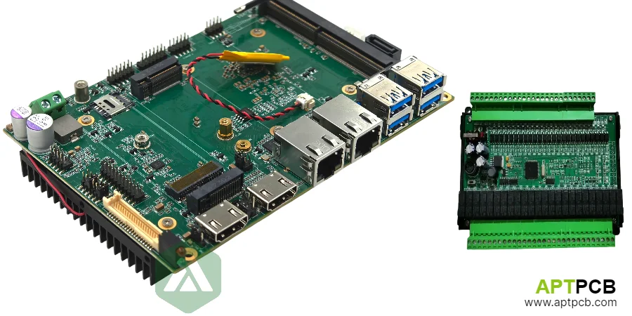
A Programmable Logic Controller executes real-time control logic while interfacing with dozens—sometimes hundreds—of field devices through digital and analog I/O channels. The PCB must maintain signal integrity across electrically hostile factory environments where motor drives, welding equipment, and switching contactors generate conducted and radiated interference continuously.
This guide covers the PCB-level engineering that determines whether a PLC operates reliably across a 20-year service life in industrial conditions—or fails unpredictably when production demands peak.
In This Guide
- I/O Isolation Architecture
- Industrial EMC and Noise Immunity
- Modular Backplane Design
- Power Distribution and Protection
- Thermal Management in Enclosures
- Manufacturing for Industrial Reliability
I/O Isolation Architecture
PLC I/O interfaces connect directly to field wiring that may carry transients exceeding 2kV during contactor switching or ground fault events. Galvanic isolation prevents these disturbances from propagating to the processor and corrupting control logic—a safety-critical requirement in industrial automation.
Optocoupler-based isolation remains common for digital I/O, with high-speed optocouplers (10+ Mbps) enabling faster scan times. The PCB layout must maintain creepage and clearance distances specified by IEC 60664-1 based on pollution degree (typically PD3 for industrial environments) and working voltage. For 24VDC I/O operating in PD3 environments, minimum creepage reaches 4mm on PCB surfaces.
Digital isolator ICs using capacitive or magnetic coupling offer higher speed and lower power than optocouplers. These devices require careful attention to common-mode transient immunity (CMTI)—the ability to reject fast common-mode voltage changes without false triggering. Industrial-grade digital isolators specify CMTI exceeding 50kV/μs.
I/O Isolation Implementation
- Creepage Distance: Maintain 4-8mm between isolated domains depending on working voltage and pollution degree per IEC 60664-1.
- Isolation Barrier Routing: No traces, copper pours, or vias cross the isolation barrier except through qualified isolation components.
- Reinforced Isolation: Safety-rated I/O uses reinforced isolation (5 kVrms isolation rating) with doubled creepage requirements.
- Ground Plane Splits: Isolated ground planes connect only through the isolation device's internal coupling mechanism.
- Transient Protection: TVS diodes and varistors on field-side I/O clamp transients before they stress isolation barriers.
- Channel-to-Channel Isolation: High-channel-count modules may require isolation between channel groups, not just field-to-logic isolation.
Industrial EMC and Noise Immunity
Factory floors present EMC challenges that dwarf typical commercial environments. Variable frequency drives generate conducted emissions from DC to tens of MHz; arc welders produce broadband impulse noise; relay coils create inductive kickback transients. The PLC PCB must reject these disturbances while meeting emissions limits that prevent interference with sensitive nearby equipment.
Conducted immunity testing per IEC 61000-4-6 requires rejection of 10Vrms RF currents injected onto I/O and power lines from 150kHz to 80MHz. Burst immunity per IEC 61000-4-4 applies 2kV fast transient bursts at 5kHz repetition rate. Surge immunity per IEC 61000-4-5 subjects the unit to 2kV line-to-ground and 1kV line-to-line surges. These tests reflect real industrial disturbances.
Power supply filtering on industrial power PCB designs combines common-mode chokes, X and Y capacitors, and ferrite beads to attenuate conducted emissions and provide immunity. Filter corner frequency must be low enough to reject industrial noise while maintaining power supply transient response.
EMC Design Strategies
- Multi-Stage Filtering: Cascaded filter stages address different frequency ranges—LC filters for low frequencies, ferrites for high frequencies.
- Shield Partitioning: Metal shields or PCB shield cans isolate sensitive analog sections from noisy digital and power circuits.
- Ground Plane Integrity: Unbroken ground planes under signal traces provide low-impedance return paths that minimize loop area.
- Connector Filtering: Filtered connectors or PCB-mount filters at I/O entry points stop noise at the boundary.
- Cable Shield Termination: 360-degree shield termination to chassis ground prevents shield currents from coupling into PCB grounds.
- Spread Spectrum Clocking: Processor and communication clocks use spread spectrum to reduce peak emissions at harmonic frequencies.
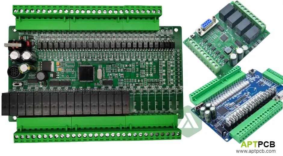
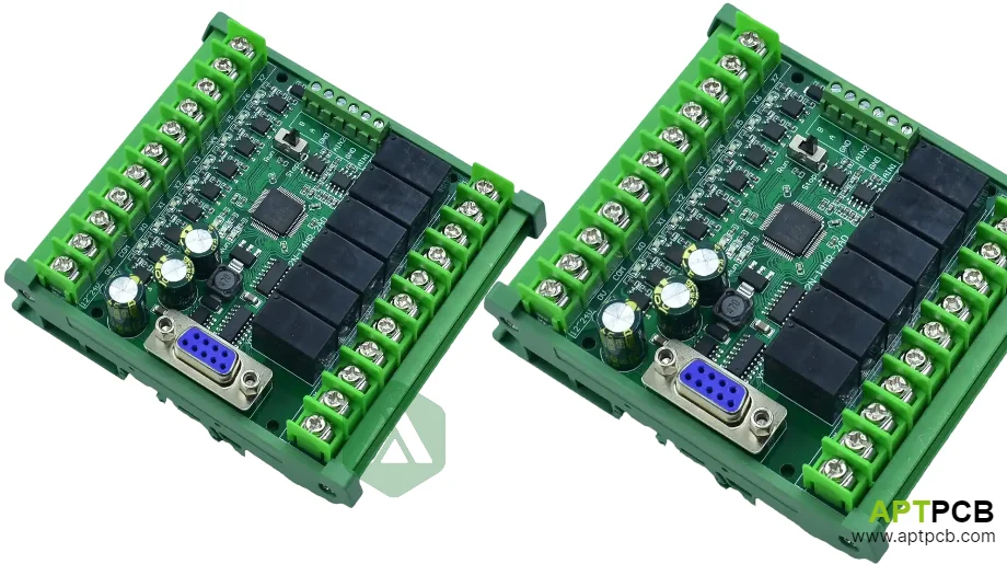
Modular Backplane Design
Modern PLCs use modular architectures where a backplane PCB interconnects processor, power supply, and I/O modules. This backplane carries high-speed digital buses, analog signals, and substantial DC power—all while enabling hot-swap capability in some systems. The multilayer PCB stackup must accommodate these diverse requirements without crosstalk or power integrity issues.
Backplane buses in current PLCs range from proprietary parallel interfaces to standard protocols like EtherCAT, PROFINET, or proprietary high-speed serial links exceeding 100Mbps. High-speed serial reduces pin count but demands controlled impedance traces and careful attention to insertion loss across backplane connectors.
Connector selection balances reliability, density, and hot-swap requirements. High-reliability connectors with gas-tight interfaces resist corrosion in industrial atmospheres. Staggered power and ground pins enable module insertion without glitching operating modules—critical for live maintenance scenarios.
Backplane Engineering Requirements
- Impedance Control: High-speed serial lanes require ±10% impedance tolerance; differential pairs need length matching within 5 mils.
- Power Distribution: Heavy copper planes (2-4 oz) distribute 24VDC backplane power to modules with minimal voltage drop.
- Connector Reliability: Industrial-grade connectors rated for 500+ mating cycles with gas-tight contacts for corrosion resistance.
- Crosstalk Management: Guard traces or ground references between high-speed and sensitive analog channels.
- Hot-Swap Sequencing: Staggered pin lengths ensure ground connects before power during module insertion.
- Mechanical Support: Backplane mounting provides adequate mechanical support for module retention under vibration.
Power Distribution and Protection
PLCs typically operate from 24VDC nominal with tolerance ranges of 20-28VDC, though some systems accept AC mains directly. The PCB power distribution network must maintain regulation under load transients while protecting against reverse polarity, overvoltage, and transient events that industrial environments generate regularly.
Input protection circuits on industrial control PCBs include reverse polarity protection (ideal diode or P-channel MOSFET), overvoltage protection (TVS or crowbar circuits), and inrush current limiting. These protections must not compromise normal operation—forward voltage drop affects efficiency, and protection response time must be faster than circuit damage thresholds.
Multi-rail power architectures serve different circuit domains: 3.3V or 5V for digital logic, ±15V or 24V for analog I/O, isolated supplies for communication interfaces. Each rail requires appropriate regulation, filtering, and sequencing to ensure reliable startup and operation.
Power System Design
- Input Protection: Reverse polarity (100V+ blocking), TVS surge suppression, resettable fuse for overcurrent.
- Inrush Limiting: NTC thermistor or active limiting prevents tripping upstream breakers during power-up.
- Regulation Efficiency: Switch-mode regulators with 90%+ efficiency minimize heat generation in enclosed installations.
- Sequencing: Power rails start in defined sequence to prevent latch-up or improper initialization.
- Bulk Capacitance: Hold-up time capacitors maintain operation during brief power interruptions (10-20ms typical).
- Monitoring: Voltage supervisors detect out-of-range conditions and trigger orderly shutdown or fault indication.
Thermal Management in Enclosures
PLCs mount in electrical enclosures where ambient temperatures may reach 55-60°C and natural convection is limited. The PCB and enclosure design must dissipate internally generated heat without relying on forced air cooling—many industrial environments prohibit fans due to dust contamination concerns.
Component placement and copper distribution on thermal management PCBs spread heat across available surface area. Power semiconductors connect to internal copper planes that conduct heat to enclosure surfaces or heatsinks. Thermal vias under components reduce junction-to-ambient thermal resistance by 30-50% compared to surface-only cooling.
Industrial temperature grades span -40°C to +85°C ambient, translating to junction temperatures exceeding 100°C under worst-case conditions. Component selection must account for derating at temperature extremes—electrolytic capacitors, in particular, suffer dramatically shortened life at elevated temperatures.
Thermal Design Approaches
- Copper Spreading: 2-4 oz copper planes conduct heat from concentrated sources to larger radiation areas.
- Thermal Via Arrays: Via arrays under power devices reduce thermal resistance to internal or bottom copper planes.
- Component Placement: Hot components positioned near enclosure surfaces or ventilation paths, not in thermal dead zones.
- Capacitor Selection: Polymer or ceramic capacitors replace electrolytics in hot zones to improve reliability.
- Conformal Coating: Consider thermal impact—some coatings impede convection while improving moisture resistance.
- Enclosure Integration: Design coordinates with enclosure manufacturer to optimize heat paths to external surfaces.
Manufacturing for Industrial Reliability
Industrial PLCs require manufacturing processes that ensure 20+ year service life with minimal field failures. This demands tighter process controls, 100% testing, and material selections that exceed typical commercial standards. The PCB fabrication and assembly processes must maintain these quality levels across production volumes.
PCB substrate selection favors high-Tg materials (Tg ≥170°C) that withstand both assembly temperatures and long-term operation at elevated temperatures. Copper adhesion and plating quality affect long-term reliability under thermal cycling—poor adhesion leads to trace lifting after thousands of thermal cycles.
Solder joint reliability depends on proper intermetallic formation, absence of voids, and appropriate fillet geometry. X-ray inspection verifies BGA and QFN solder joints that visual inspection cannot assess. Functional testing validates I/O isolation, analog accuracy, and communication interfaces before shipment.
Manufacturing Quality Requirements
- IPC Class 3: Industrial electronics require Class 3 workmanship per IPC-A-610 for highest reliability.
- Solder Joint Inspection: 100% AOI with statistical X-ray sampling for hidden joints.
- Burn-In Testing: Optional accelerated life testing catches infant mortality failures before shipment.
- Conformal Coating: Selective coating protects against moisture and contamination while leaving thermal paths clear.
- Traceability: Full component and process traceability enables root cause analysis if field failures occur.
- Environmental Testing: Sample testing per IEC 60068 validates temperature, humidity, and vibration performance.
Summary
PLC PCB design balances the conflicting demands of noise immunity, thermal management, modular flexibility, and long-term reliability. Success requires understanding industrial environment realities—transient events measured in kilovolts, ambient temperatures that challenge component ratings, and service life expectations spanning decades. The PCB engineering decisions made during design determine whether the PLC performs reliably throughout its intended lifecycle or becomes a maintenance burden that disrupts production.