The bare board is done. It has passed TDR impedance testing, microsection inspection, and Rogers material lot verification. Now it goes into SMT assembly—and the assembly process introduces a second set of failure modes that the fabrication process can't prevent.
RO3003 PCB assembly is technically more demanding than standard FR-4 assembly in four specific areas: moisture management before line entry, solder paste stencil design for thermal pad via structures, reflow atmosphere and temperature profile, and post-assembly inspection of hidden solder joints. Each one has a defined best practice. Skipping any one of them shows up as voiding under the thermal pad, delamination at the PTFE/FR-4 hybrid interface, or solder joint failures that appear within the first hundred thermal cycles.
This guide covers all four in detail—what the problem is, what the process solution looks like, and what the acceptance criteria are.
Four Assembly Variables That FR-4 Process Settings Can't Handle
Before covering individual assembly steps, it's useful to understand exactly what about RO3003 makes standard FR-4 assembly parameters inadequate—not just "different," but actively failure-inducing.
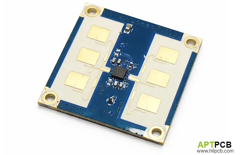
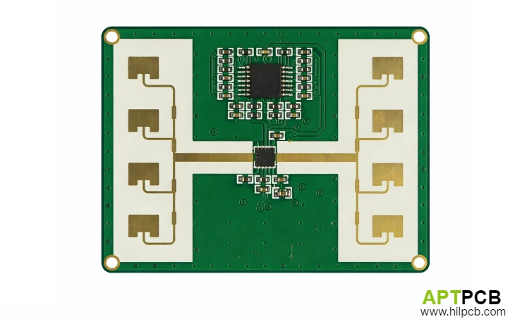
Immersion Silver surface finish. Most RF-optimized RO3003 boards arrive with ImAg surface finish—the preferred choice because its thin, flat deposit is electromagnetically transparent at high frequencies. Unlike ENIG, ImAg tarnishes when exposed to sulfur compounds or elevated temperatures. It requires nitrogen reflow atmosphere and precise thermal profiling that standard FR-4 assembly lines running air reflow don't provide.
Hybrid substrate moisture sensitivity. Even though RO3003 itself absorbs almost no moisture (0.04%), the FR-4 inner layers of a hybrid board are hygroscopic. Moisture that migrates to the RO3003/FR-4 bonding interface during a 250°C reflow cycle can flash to steam, causing internal delamination. Pre-bake protocols must address the FR-4 layers, not just treat the board as a single-material unit.
POFV thermal via arrays. Plated-over-filled vias beneath RF transceiver thermal pads create a specific SMT challenge: paste printed over a via array can collapse into the barrels during reflow if stencil aperture design doesn't account for it. The voiding consequence is a blocked thermal path that no amount of rework can restore. At the design stage, how the via is filled and capped determines how flat the landing surface is—which directly affects paste deposit uniformity over the array. Boards where the POFV cap plating is not flush with the pad surface will show predictable voiding at the depressed zones regardless of stencil geometry.
Lower peak reflow temperature ceiling. PTFE's thermal expansion behavior at temperatures above 250°C begins to stress the interface between the PTFE matrix and copper via barrel plating in ways that don't apply to FR-4 boards. This constrains the reflow profile in ways described in detail below.
Understanding these constraints at the assembly planning stage—not after the first 3D X-ray run—is what separates high-yield RO3003 assembly from expensive rework cycles.
Moisture Pre-Bake: Protecting the Hybrid Interface Before Reflow
The Physics of Steam Delamination
FR-4's standard moisture absorption rate is approximately 0.1–0.5% by weight after exposure to normal ambient conditions. For a hybrid board that spent time in an uncontrolled warehouse, traveled in a container, or simply sat in incoming inspection for several days, FR-4 inner layers can absorb moisture from the air through any exposed board edge.
During reflow, when the board climbs through the 200–250°C range, absorbed water at the FR-4/RO3003 bonding interface converts to steam. The volumetric expansion is dramatic. If the steam can't escape before the solder solidifies and the board cools, the resulting pressure creates delamination blisters at the hybrid bond line—visible in cross-section as a separation between the RO3003 outer layer and the FR-4 core.
This is a reliability-ending defect. The delaminated board passes all solder joint inspection. It fails thermally because the FR-4/RO3003 interface is no longer mechanically continuous.
Pre-Bake Protocol
APTPCB pre-bakes all hybrid RO3003/FR-4 boards immediately before SMT line entry. The bake cycle drives absorbed moisture from FR-4 layers without aggressively oxidizing the ImAg surface finish—a temperature/time trade-off that requires characterization for each board construction type.
After bake completion, boards enter the SMT line within minutes. Re-exposure to ambient air between bake and reflow reintroduces moisture; the pre-bake value is consumed if boards wait at room temperature for hours before entering the line.
For programs where the pre-bake-to-reflow window cannot be controlled (boards baked at one facility, assembled at another), the safest approach is to keep boards sealed in their moisture barrier bags until line entry and schedule bake immediately before placement—coordinating bake completion with machine setup time, not with the work order schedule.
Window-Pane Stencil Design: Eliminating Thermal Pad Voiding
Why Full-Aperture Stencils Fail on Thermal Pads
A standard stencil aperture for a QFN thermal pad prints a single continuous solder deposit covering the full pad area. During reflow, flux chemistry in the solder paste activates, performs its cleaning function on the copper surface, and needs to outgas through the molten solder. On a large, flat pad with a single continuous paste deposit, that flux vapor has nowhere to go—it nucleates as voids beneath the molten pool and remains trapped as the solder solidifies.
On RO3003 boards with POFV arrays beneath the thermal pad, the situation is worse: voids directly over via columns block the primary thermal extraction path. A single large void over a cluster of copper via barrels can increase local junction temperature significantly above what the thermal design predicted. That margin loss directly affects RFIC reliability under thermal cycling.
Window-Pane Aperture Design
The window-pane stencil divides the thermal pad aperture into a grid of smaller segments separated by paste-free web strips, typically 0.15–0.20mm wide. The principle: during reflow, flux vapor escapes through the web strip openings before solder solidifies. Multiple small paste deposits coalesce as the solder melts but the escape channels remain open long enough to allow outgassing.
Window-pane parameters for RO3003 thermal pad structures:
- Individual aperture segment area: ≤1.5 × 1.5mm
- Web strip width: 0.15–0.20mm
- Total paste coverage: 50–80% of thermal pad area
- Stencil thickness: 0.12–0.15mm (consistent with adjacent peripheral pads)
This aperture geometry, combined with nitrogen reflow atmosphere (next section), consistently produces thermal pad voiding below 10% on properly designed POFV arrays. To be precise on the numbers: IPC-A-610 Class 3 sets the acceptance limit at 30% aggregate voiding; APTPCB's internal acceptance threshold is tighter at 20%. The under-10% figure is the actual process capability achieved in production with this stencil geometry—it is what the process delivers, not the limit it is judged against.
Nitrogen Reflow: Atmosphere, Profile, and Temperature Targets
Why Nitrogen Is Required for ImAg/RO3003 Assembly
Air reflow at RF module assembly temperatures introduces two failure mechanisms:
ImAg tarnishing. Immersion Silver oxidizes under elevated temperature in an oxygen-containing atmosphere. A tarnished ImAg surface loses solderability—solder doesn't wet consistently, producing open joints or high-void solder coverage on pads that appeared clean before reflow.
Solder powder oxidation. Solder paste particles develop surface oxide films during the ramp phase when the oven atmosphere contains oxygen. These oxide films increase the solder's viscosity during reflow, reduce wetting force, and promote void formation in all solder joints—not just thermal pads.
APTPCB's reflow ovens for RO3003 RF modules operate with pure nitrogen atmosphere at residual oxygen below 500 ppm. At this oxygen level, ImAg surface oxidation is negligible through the full thermal cycle, and solder paste wetting is markedly better than air reflow.
Reflow Profile for RO3003 Hybrid Boards
| Stage | Target | Constraint |
|---|---|---|
| Preheat ramp | 1.5–2°C/second | Ramp too fast: thermally shocks FR-4/RO3003 interface |
| Soak zone (flux activation) | 150–180°C, 60–90 seconds | Insufficient soak: incomplete flux activation, void formation |
| Peak temperature | 245–250°C | Maximum 260°C; lower peak reduces PTFE/copper interface stress |
| Time above liquidus (183°C) | 30–45 seconds | Longer: increases thermal stress; shorter: incomplete coalescence |
| Cooling rate | ≤3°C/second | Faster: thermal shock to hybrid bond line |
The 245–250°C peak is lower than the 255–260°C common on FR-4 lines. The reduction is deliberate: PTFE's thermal expansion behavior at temperatures above 250°C begins to stress the interface between the PTFE matrix and the copper via barrel plating. Lower peak temperature, with adequate time above liquidus for full solder coalescence, produces better long-term joint reliability on RO3003 substrates.
Multiple reflow passes above 220°C should be limited to two where possible. If rework requires a third pass, evaluate the assembled board for PTFE/FR-4 interface integrity before returning to service.
Component Placement Considerations for RF Transceivers
Thermal Pad Co-planarity
QFN and chip-scale RF ICs typically have an exposed thermal pad that must make uniform contact with the POFV solder deposit. Co-planarity of the component package—the variation in terminal height across the package—must be within the solder paste deposit height to ensure the thermal pad contacts the paste consistently.
Before line entry, verify component co-planarity is within 0.05mm. Components exceeding this threshold produce non-uniform thermal pad contact, with predictable voiding at the elevated corner(s) even with correct window-pane stencil design.
Fine-Pitch RF Connector Pads
Many RF modules include edge-launch RF connectors for test access. These typically have 0.5mm or smaller pitch. On RO3003 boards with ImAg finish, the flatness of the surface finish is an advantage—ImAg's thin, planar deposit doesn't create the height variation that HASL would. These fine-pitch structures require solder paste print inspection (SPI) before placement to confirm paste volume and registration before any component is placed.
Underfill Considerations for Harsh Environments
RF modules operating in harsh environments—automotive exterior, outdoor base station, or airborne applications—experience vibration levels and thermal shock rates that can exceed the solder joint fatigue life of large BGA packages without underfill. Where BGA components are used on RO3003 boards, the underfill material selection requires consideration of adhesion to the ImAg surface and compatibility with the RO3003 dielectric—not all underfill formulations wet PTFE-based substrates adequately.
3D X-Ray Inspection: The Only Way to See What Matters
What AOI Misses
After reflow, standard Automated Optical Inspection (AOI) cameras photograph the assembly from above. For QFN RF transceivers—with all solder joints hidden beneath the package body, BGAs with solder balls completely enclosed, and exposed thermal pads visible only through the component—AOI sees nothing relevant. The components that matter most on a high-frequency RF board are exactly the components AOI is blind to.
2D X-ray is an improvement but insufficient for POFV structures: a 2D projection collapses the via copper columns, the solder layer above them, and the board layers below into a single image. Measuring void area in the solder layer in isolation is not possible.
3D AXI with Computed Tomography
APTPCB's 3D Automated X-Ray Inspection systems reconstruct a high-resolution volumetric model from multi-angle projections. Quality engineers slice through the exact plane of the solder layer—isolated from via copper above and board layers below—and measure:
- Total aggregate void percentage across the thermal pad
- Individual void dimensions and positions
- Void proximity to POFV via columns
APTPCB's RO3003 Assembly Voiding Acceptance Criteria:
| Criterion | IPC-A-610 Class 3 | APTPCB Internal |
|---|---|---|
| Total thermal pad voiding | ≤30% | ≤20% |
| Any single void | Not specified | ≤5% of pad area |
| Any void over a POFV thermal via | Not specified | Zero tolerance |
The zero-tolerance criterion for voids over thermal vias is not in IPC-A-610—it's an APTPCB-specific requirement derived from thermal simulation. A void directly over a filled copper via column severs the primary heat path from the RFIC junction to the chassis. Operating above maximum junction temperature is the result; the failure mode is gradual gain compression followed by device failure. No design margin can compensate for a broken thermal path.
First Article Inspection for RO3003 Assembly Programs
Before production runs are released, APTPCB conducts First Article Inspection (FAI) on RO3003 assembly programs. FAI for an RF module includes:
- 100% 3D AXI on all bottom-terminated components
- Microsection cross-section of a representative solder joint set (thermal pad + peripheral pads)
- Thermal resistance measurement on the RFIC thermal path (if test access permits)
- Reflow profile documentation for the specific board/oven combination
- Solder paste SPI data from the first production print cycle
FAI documentation becomes the baseline against which production lot sampling is measured. If voiding trends upward in production sampling, the FAI data identifies whether the deviation is in stencil performance, paste volume, or oven profile—without having to reverse-engineer the root cause from scratch.
Why Fabrication and Assembly Integration Matters for RO3003
The most reliable way to execute RO3003 PCB assembly is to not separate it from fabrication. When bare board fabrication and SMT assembly are performed by the same team in the same facility:
- Pre-bake timing is controlled by the same schedule that manages line loading
- ImAg shelf life is managed with direct knowledge of the board's fabrication date
- POFV surface planarity data from fabrication is available to the assembly engineer who designs the stencil apertures
- 3D AXI voiding results feed directly back to the fabrication team as a process performance indicator
When fabrication and assembly are split across two suppliers, accountability for voiding failures fragments: the assembly vendor attributes it to POFV planarity or ImAg degradation during shipping; the fabricator attributes it to the reflow profile. The OEM holds the liability and the schedule delay.
APTPCB's turnkey service covers Rogers RO3003 PCB fabrication through SMT assembly with shared DFM documentation, co-located storage, and a single IATF 16949 quality management system covering both process stages.
If your program has already encountered unexpected voiding in production—or if you're evaluating the stencil design before your first prototype run—the quickest diagnostic path is to compare 3D AXI slice data against the FAI baseline and cross-reference it with pre-bake timing records. Most persistent voiding problems on RO3003 programs trace back to one of three variables: pre-bake-to-reflow interval drift, ImAg age since fabrication, or stencil wear over production. Contact our assembly engineering team with your 3D AXI data and we can typically identify the root cause before a new stencil is ordered.
References
- SMT void acceptance per IPC-A-610 Acceptability of Electronic Assemblies, Class 3.
- Reflow profile and nitrogen atmosphere guidance from APTPCB High-Frequency SMT Assembly Control Plan (2026).
- Moisture pre-bake requirements per IPC-1601 Printed Board Handling and Storage Guidelines.
- POFV requirements per IPC-4761 Design Guide for Protection of Printed Board Via Structures.