Set-top boxes and streaming media devices represent one of the highest-volume consumer electronics categories, with tens of millions of units shipped annually by major manufacturers. The PCB design challenge centers on achieving adequate performance for 4K video streaming and gaming while meeting aggressive cost targets—typical retail prices under $50 require BOM optimization at every level.
This guide examines set-top box PCB design requirements: implementing streaming SoCs with integrated functionality, optimizing HDMI output signal quality, integrating WiFi and Bluetooth connectivity, achieving thermal targets within compact fanless enclosures, and manufacturing strategies that balance quality against volume cost optimization.
In This Guide
- Streaming SoC Implementation and Memory Interface
- HDMI Output Design for 4K Video Quality
- WiFi and Bluetooth Antenna Integration
- Thermal Management in Fanless Enclosures
- High-Volume Manufacturing Optimization
- Testing and Quality Assurance for Volume Production
Streaming SoC Implementation and Memory Interface
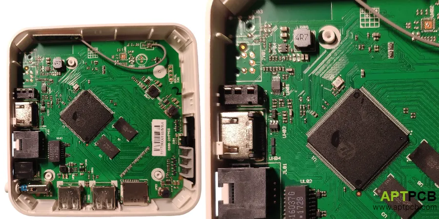
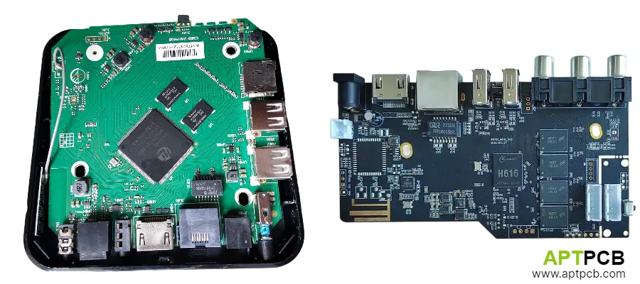
Modern set-top box SoCs integrate CPU cores, GPU, video decoder, HDMI transmitter, USB, and often WiFi/Bluetooth into single-chip solutions from vendors like Amlogic, Realtek, and Rockchip. These highly integrated devices simplify board design but require careful attention to memory interface routing and power delivery to achieve reliable operation across production variation.
Memory configurations typically range from 1-4GB DDR3/DDR4 in cost-sensitive designs to LPDDR4 in premium devices. The memory interface often determines PCB layer count requirements—DDR4 at speeds above 2400 MT/s requires routing discipline that may exceed 4-layer capability, while lower-speed DDR3 configurations can achieve adequate performance with simpler stackups.
SoC and Memory Implementation
- Package Considerations: Set-top box SoCs typically use 0.65-0.8mm pitch BGAs with 300-600 pins; standard via-in-pad or dog-bone fanout achieves routing without HDI.
- Memory Topology: Most SoCs use single-rank memory configuration; point-to-point topology from SoC to single memory IC simplifies routing versus multi-rank designs.
- Speed Selection: DDR4-2133 or DDR4-2400 provides adequate bandwidth for 4K streaming at moderate cost; higher speeds add cost without perceptible performance benefit for typical use cases.
- Length Matching: DDR interface requires matched routing—DQ signals within byte lane ±5mm; DQS-to-DQ ±2mm; address/command to clock ±25mm depending on SoC specification.
- Impedance Requirements: Typical DDR4 impedance targets: 40Ω for single-ended data/address, 80Ω differential for clock; ±10% tolerance achievable with standard processes.
- Termination: On-die termination (ODT) handles most termination requirements; external termination rarely needed for single-rank configurations.
Simple memory interfaces often succeed with multilayer PCB construction using standard 4-6 layer stackups without advanced HDI requirements.
HDMI Output Design for 4K Video Quality
HDMI output quality directly affects user perception of device quality—visible artifacts, color banding, or audio dropouts suggest inferior device quality regardless of actual streaming performance. Set-top boxes typically output HDMI 2.0 (18 Gbps, supporting 4K60 HDR) from integrated transmitter in the SoC, requiring PCB routing that maintains signal integrity from silicon through connector.
The cost optimization pressure in set-top box design creates temptation to minimize HDMI routing investment—short traces, standard materials, relaxed impedance tolerances. Within limits, these simplifications work; pushed too far, they result in marginal HDMI performance that causes intermittent issues with certain TVs or cable lengths.
HDMI Output Routing
- Trace Length: Keep HDMI traces under 75mm from SoC to connector; shorter traces tolerate process variation better and reduce high-frequency loss.
- Impedance Target: 100Ω differential impedance ±15% sufficient for HDMI 2.0 at moderate trace lengths; tighter tolerance for longer traces or HDMI 2.1.
- Layer Selection: Microstrip routing on outer layer acceptable for short traces with proper ground reference; stripline provides better EMI containment.
- Connector Quality: HDMI connector selection affects both signal integrity and mechanical reliability; cost optimization should not sacrifice connector quality—field failures from poor connectors exceed savings.
- ESD Protection: TVS diodes at HDMI connector protect against static discharge; select low-capacitance devices (<0.5pF) to minimize signal degradation.
- AC Coupling: HDMI specification requires AC coupling on data lanes; 100nF capacitors in 0402 size placed close to SoC output pins.
HDMI routing for standard HDMI 2.0 typically succeeds with basic design discipline without requiring specialized high-speed techniques, but verification against specification compliance ensures reliable operation.
WiFi and Bluetooth Antenna Integration
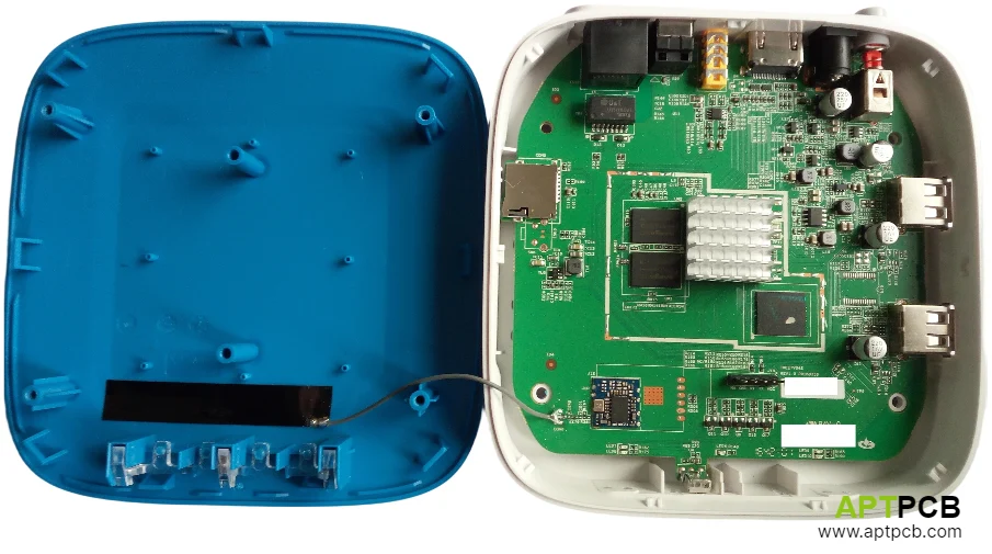
WiFi connectivity is essential for streaming devices—performance directly affects user experience through buffering, quality adaptation, and connection reliability. Most set-top box designs use integrated WiFi modules (SoC with built-in wireless or separate WiFi SoC) with on-board antennas, requiring careful RF layout and antenna placement within compact enclosures.
Antenna performance in small enclosures depends heavily on ground plane design, keep-out regions, and enclosure material properties. Metal enclosures (common in premium designs) require external antennas or carefully-designed apertures for antenna radiation, while plastic enclosures allow internal antennas with proper clearance design.
Wireless Integration Considerations
- Module Selection: Integrated WiFi (SoC with built-in radio) minimizes cost but limits flexibility; discrete WiFi modules offer certified performance and multiple supplier options.
- Antenna Types: PCB-printed antennas minimize cost but require ground plane optimization; chip antennas provide consistent performance in smaller area; external antennas for metal enclosures.
- 2.4GHz vs. 5GHz: Dual-band designs require either dual-band antenna or separate antennas; single-band 5GHz provides better streaming performance in congested environments.
- Ground Plane Clearance: PCB antennas require ground-free region extending from antenna element; dimensions depend on frequency and antenna type—typically 10-15mm for chip antennas.
- RF Trace Routing: 50Ω microstrip from wireless IC to antenna; keep traces short and avoid vias in RF path; controlled impedance essential for antenna matching.
- Enclosure Effects: Plastic enclosure materials affect antenna tuning; prototype with production enclosure material for accurate performance assessment.
Wireless performance optimization benefits from antenna PCB design expertise and RF measurement capability for tuning and verification.
Thermal Management in Fanless Enclosures
Consumer preference for silent operation drives fanless set-top box designs, requiring the PCB and enclosure to dissipate SoC power (typically 3-8W during 4K playback) through conduction and natural convection. The compact enclosures (often under 150mm × 100mm × 25mm) limit heat spreading area, making thermal design critical for sustained performance without throttling.
The PCB serves as the primary heat spreader in most set-top box thermal designs. Heat conducts from SoC through thermal vias to copper planes, spreads laterally across the board, and transfers to enclosure through thermal pads or direct contact. Enclosure surface area then dissipates heat through convection and radiation.
Thermal Design Strategies
- Thermal Via Array: Dense via array (0.3mm drill, 0.5mm pitch) beneath SoC package conducts heat to inner layers and bottom surface; filled vias preferred to prevent solder wicking.
- Copper Coverage: Maximize copper pour on all layers beneath and around SoC; ground planes serve double duty for electrical return and thermal spreading.
- Top-side Heat Sink: Aluminum spreaders or heat sinks attached to SoC top surface provide additional thermal path; thermal interface material bridges gap between component and spreader.
- Bottom-side Thermal Path: Heat transfer to enclosure bottom through thermal pads or direct board contact; requires flat copper area without vias or component intrusion.
- Component Placement: Keep heat-generating components (regulators, wireless ICs) away from SoC to prevent thermal interaction; distribute heat sources across board area.
- Enclosure Design: Enclosure material conductivity affects system thermal performance; aluminum enclosures provide excellent heat spreading; plastic enclosures rely more on convection.
Thermal simulation during design phase identifies hot spots and validates thermal solution adequacy before physical prototyping, saving development time and iteration cycles.
High-Volume Manufacturing Optimization
Set-top box volumes—often hundreds of thousands to millions of units annually—justify manufacturing optimization investments that lower-volume products cannot support. PCB design decisions directly affect manufacturing cost through panel utilization, layer count, material selection, and test coverage. Every cent saved on PCB cost multiplied by volume becomes significant.
Cost optimization requires balancing multiple factors: layer count reduction saves material cost but may require more complex routing or larger board size; standard materials cost less but may limit performance; smaller boards improve panel utilization but constrain component placement and thermal spreading.
Manufacturing Cost Factors
- Layer Count: 4-layer designs significantly cheaper than 6-layer; 2-layer possible for simplest designs—each layer pair adds ~20-30% to board cost.
- Material Selection: Standard FR-4 (Tg 130-150°C) suits most applications; higher-Tg materials only if assembly reflow profiles require—no performance benefit otherwise.
- Board Size Optimization: Smaller boards improve panel utilization; standardize dimensions across product variants to share panel layout optimization.
- Via Structure: Through-hole vias only (no blind/buried) for cost-sensitive designs; HDI adds significant cost—reserve for unavoidable fine-pitch routing.
- Surface Finish: HASL lowest cost for standard assembly; ENIG/OSP for fine-pitch requirements—specify appropriately rather than over-specifying.
- Panel Design: Work with manufacturer on optimal panel layout; edge rails, scoring versus routing, and test coupon placement affect utilization and handling.
Volume manufacturing partnerships through mass production PCB services enable economies of scale that reduce per-unit costs while maintaining quality standards.
Testing and Quality Assurance for Volume Production
High-volume set-top box production requires efficient testing strategies that catch defects without becoming cost or throughput bottlenecks. The testing approach must balance defect detection against test cost—exhaustive testing that catches every possible defect but adds significant cost per unit may not optimize total cost (production plus warranty).
Effective test strategies combine in-circuit testing (ICT) or flying probe for electrical verification, functional testing for operational verification, and automated optical inspection (AOI) for assembly defect detection. Design for test (DFT) principles incorporated during PCB design enable efficient test implementation.
Test Strategy Components
- In-Circuit Test (ICT): Fixture-based testing provides fast, comprehensive electrical verification; requires test pad access—design test points at appropriate locations.
- Flying Probe: Fixture-less alternative for lower volumes or board variants; slower than ICT but eliminates fixture cost and lead time.
- Functional Test: Power-up testing verifies operation; HDMI output test, WiFi connection test, video playback verification confirm system functionality.
- Automated Optical Inspection: AOI verifies solder joint quality, component presence/orientation; catches assembly defects that electrical tests might miss.
- Test Coverage Trade-offs: 100% node coverage often impractical; prioritize high-risk nets (power, critical signals) and accept reduced coverage on low-risk areas.
- Defect Tracking: Statistical analysis of test failures identifies process issues; closed-loop feedback improves both assembly and test processes.
Comprehensive test and quality systems ensure production quality while optimizing test efficiency for high-volume manufacturing economics.
Technical Summary
Set-top box PCB design exemplifies the challenge of achieving adequate performance within aggressive cost constraints—volumes measure in millions of units, but retail prices under $50 require optimization at every level. Success requires making appropriate trade-offs: simplified where performance margins permit, disciplined design where critical (HDMI output, wireless performance, thermal management).
Key decisions in set-top box development include layer count (4-layer versus 6-layer based on routing complexity), material selection (standard versus enhanced FR-4 based on thermal and performance requirements), wireless integration approach (integrated versus module, antenna type), and thermal solution (board design role in system thermal management).
Manufacturing partner selection should emphasize high-volume capabilities, cost competitiveness, and quality systems—set-top box volumes justify supplier optimization, but warranty costs from quality issues quickly eliminate manufacturing savings. Early engagement enables design-for-manufacturing optimization that benefits both quality and cost.