Smart TV main boards integrate application processing, video scaling and processing, multiple high-speed interfaces (HDMI, USB, Ethernet), wireless connectivity, and audio systems onto boards that must meet aggressive cost targets while delivering premium viewing experiences. The PCB design challenges span from ultra-high-speed HDMI 2.1 interfaces (48 Gbps aggregate) to large panel driving interfaces and power supply integration.
This guide covers the PCB-specific considerations for smart TV design: board partitioning between main board and T-CON, video processing SoC routing requirements, HDMI 2.1 signal integrity, panel interface design, power supply architecture, and the manufacturing balance between quality and cost optimization essential for television products.
Design Checklist (Fast Pass)
- Partition early: main board vs T‑CON vs PSU board, and lock the interconnect + connector choice.
- Place HDMI close: keep HDMI 2.1 FRL paths short; plan ESD/CMC/retimer footprints up front.
- Treat DDR as a system: stackup + impedance + length matching + reference planes + return paths.
- Design the PDN + thermal together: copper, via arrays, and chassis heat‑spreading are part of the “power design”.
- DFM for cost: avoid HDI where you don’t need it; optimize panel utilization and test access.
In This Guide
- TV Board Architecture: Main Board and T-CON Partitioning
- Video Processing SoC Routing Requirements
- HDMI 2.1 High-Speed Interface Implementation
- Panel Timing Interface Design
- Power Supply Integration and Thermal Considerations
- Cost-Optimized Manufacturing for Television Products
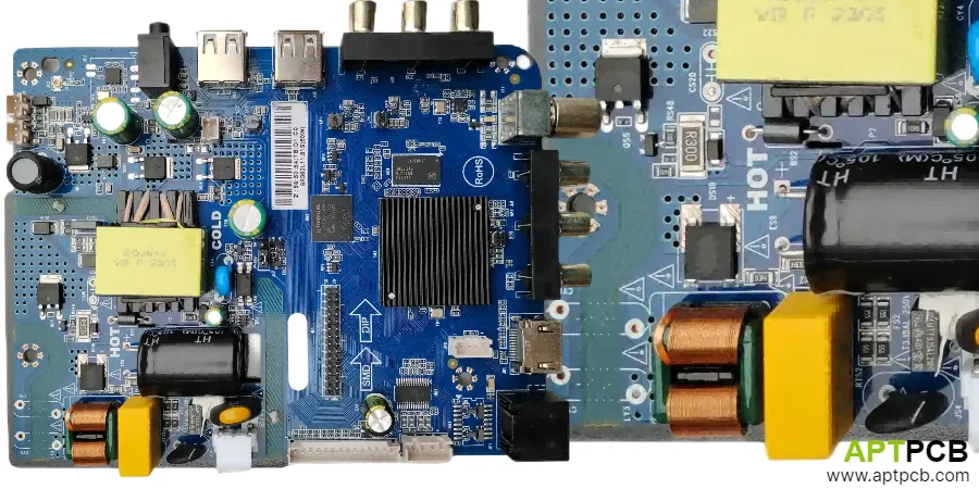
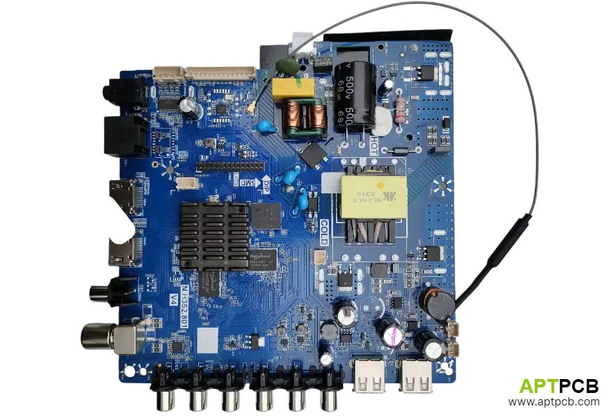
TV Board Architecture: Main Board and T-CON Partitioning
Smart TV electronics typically partition across multiple PCBs: the main board handles application processing, connectivity, and video input/processing; the T-CON (timing controller) board manages panel driving and image optimization; and the power supply board provides multiple voltage rails. This partitioning reflects both functional requirements and supply chain considerations—different panels use different T-CON designs, while main boards standardize across product lines.
The interface between main board and T-CON carries fully processed video data at resolutions up to 8K—demanding either extremely high-bandwidth parallel interfaces (LVDS requiring dozens of pairs) or serialized protocols (V-by-One, eDP) that reduce conductor count but require multi-gigabit signal integrity. This inter-board interface often determines system video performance ceiling.
Board Partitioning Considerations
- Main Board Scope: SoC, memory, HDMI receivers, USB/Ethernet interfaces, WiFi/Bluetooth modules, audio processing, and interfaces to T-CON and power boards.
- T-CON Integration Level: Some panels integrate T-CON onto the panel itself (panel-integrated driver); others use separate T-CON board—affects main board interface requirements.
- Interface Selection: Panel specs drive the choice. Many 4K60 designs use V-by-One HS with ~8 lanes in the ~3–4 Gbps/lane class; 8K usually needs more lanes/higher rates or a different interface.
- Connector Types: High-speed interfaces use specialized connectors maintaining impedance matching; ribbon cables limit bandwidth and require careful design.
- Power Distribution: Main board may provide power to T-CON (increasing main board current handling) or T-CON may receive power directly from power supply board.
- Physical Layout: Main board typically mounts at screen rear bottom area; thermal considerations require clearance from panel and adequate ventilation paths.
Understanding the system-level architecture guides PCB partitioning decisions that affect both electrical performance and manufacturing efficiency.
Video Processing SoC Routing Requirements
Smart TV SoCs integrate substantial complexity—quad-core or octa-core application processors, dedicated video decoders supporting multiple codecs at 4K/8K resolution, display engines with scaling and enhancement, and numerous interfaces. These highly-integrated devices come in large BGA packages (often 500-1000+ pins) with fine pitch (0.4-0.65mm), requiring careful PCB routing to achieve performance while maintaining manufacturability.
Memory interfaces present particular challenges—DDR4 or LPDDR4/5 at speeds demanding careful length matching and impedance control. Unlike smartphones where memory integrates into package-on-package configurations, TV SoCs typically use discrete memory requiring board-level routing with associated signal integrity considerations.
SoC Routing Guidelines
- BGA Fanout Strategy: Fine-pitch BGA requires via-in-pad or dog-bone routing; through-hole vias limit routing channels—consider blind vias for dense packages.
- Memory Interface Routing: DDR4 at 2666-3200 MT/s requires matched-length routing within byte lanes (±5mm), DQS-to-DQ matching (±10mm), and consistent impedance.
- Reference Plane Requirements: Memory and high-speed interface signals need uninterrupted reference planes; avoid routing power traces or placing vias in plane areas beneath critical signals.
- Decoupling Strategy: SoC power pins require local decoupling (100nF at each power pin cluster) plus bulk capacitance (10-100μF) nearby; place capacitors as close to pins as routing permits.
- JTAG and Debug Access: Debug interfaces (JTAG, UART) should remain accessible for development and production testing; locate test points or headers appropriately.
- Thermal Design: SoC power dissipation (5-15W typical) requires thermal vias beneath package and adequate copper spreading to heat sink mounting points.
Video processing SoC routing benefits from high-speed design techniques to ensure memory and display interfaces achieve required performance margins.
HDMI 2.1 High-Speed Interface Implementation
HDMI 2.1 represents one of the most demanding consumer interface specifications—12 Gbps per lane across four data lanes (48 Gbps aggregate) supports 8K at 60Hz or 4K at 120Hz with HDR. The PCB routing from HDMI receiver IC to connector must maintain signal integrity at frequencies where wavelengths become comparable to trace lengths, requiring transmission line design discipline.
Legacy HDMI 1.4/2.0 (up to 18 Gbps aggregate) used source-terminated differential signaling with moderate impedance tolerance. HDMI 2.1 FRL (Fixed Rate Link) raises the bar—keep 100Ω differential impedance (±10%), tightly match lengths within each differential pair, and manage insertion/return loss across the full channel (connector + PCB + cable).
HDMI 2.1 Routing Requirements
- Impedance Control: 100Ω differential impedance ±10%; tight-coupled differential pairs reduce EMI and maintain common-mode rejection.
- Channel Loss: At 12 Gbps/lane, loss margin can disappear fast. Keep traces short; if you can’t, consider low-loss laminates and/or a redriver/retimer.
- Length Constraints: Keep HDMI traces as short as practical; under 50mm minimizes loss and skew accumulation—connector placement near receiver IC important.
- Layer Selection: Route HDMI on layers adjacent to solid ground planes; microstrip on outer layers acceptable if EMI managed; stripline provides better shielding.
- Via Transitions: Avoid layer changes if possible. When unavoidable, minimize stubs (e.g., backdrill where it makes sense) and keep reference planes continuous.
- ESD Protection: HDMI ports require ESD protection; protection device placement affects signal integrity—use low-capacitance TVS diodes (<0.3pF) and place at connector.
HDMI 2.1 implementation may require signal integrity simulation to verify routing achieves compliance margins, particularly for longer trace lengths or when using standard FR-4 materials.
Panel Timing Interface Design
The interface between main board (or T-CON) and LCD/OLED panel carries video data at rates matching pixel clock and color depth. A 4K panel at 60Hz with 10-bit color requires approximately 17 Gbps of video data—delivered via LVDS, V-by-One, or proprietary interfaces depending on panel manufacturer and resolution.
V-by-One HS dominates current 4K TV implementations, using fewer lanes than LVDS (8 pairs typical versus 16-32 pairs) at higher speeds (typically 3.6-4.0 Gbps per lane). The reduced lane count simplifies routing but increases per-lane signal integrity requirements. Panel flex cable connections introduce impedance discontinuities that must be managed through connector selection and PCB termination design.
Panel Interface Implementation
- Protocol Selection: Panel specification dictates interface—V-by-One HS for most 4K panels; LVDS remains common for lower resolutions; some 8K panels use proprietary high-speed interfaces.
- Lane Configuration: V-by-One HS typically uses 8 lanes for 4K 60Hz 10-bit; lane count scales with resolution, refresh rate, and color depth.
- Connector Interface: Panel interface connectors must maintain impedance matching; flex cable routing between board and panel introduces loss and skew that affects maximum achievable bit rate.
- Reference Clock: Panel interfaces require stable reference clocks; crystal or oscillator selection, power supply filtering, and routing isolation all affect clock jitter performance.
- Termination Design: On-chip termination standard for V-by-One receivers; verify panel input termination requirements and match source output impedance.
- EMI Considerations: Panel interface signals can radiate from flex cables; proper connector grounding, cable shielding, and routing away from sensitive circuits reduces EMI impact.
Panel interface design requires close coordination with panel suppliers to verify timing, voltage levels, and connector compatibility.
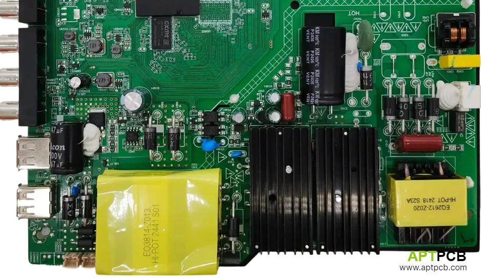
Power Supply Integration and Thermal Considerations
Smart TV main boards typically receive 5V or 12V from the power supply board, generating local rails for SoC (typically 0.9-1.1V core, plus I/O voltages), memory (1.2V for DDR4/LPDDR4), and various I/O systems. The power delivery network must support SoC transient currents while maintaining voltage regulation within tight tolerances—typically ±3% for core voltage rails.
Thermal management on TV main boards differs from portable devices—larger board area allows heat spreading, but enclosed chassis and desire for fanless operation limits cooling. The PCB serves both as mounting substrate and primary heat spreader, with heat dissipating to metal chassis through thermal interface materials.
Power and Thermal Design
- DC-DC Efficiency: Multi-phase buck converters for SoC power achieve >90% efficiency; inductor and MOSFET selection affects both efficiency and thermal performance.
- Voltage Sequencing: SoC requires specific power-up sequence (typically core, then I/O, then memory); sequencing controller or integrated PMIC provides proper timing.
- Decoupling Network: SoC PDN requires bulk capacitance (MLCC, polymer, or electrolytic), mid-frequency ceramics, and high-frequency ceramics distributed across the network.
- Copper Coverage: Maximize copper pour on inner layers beneath SoC and power conversion stages; 1oz or 2oz copper on power layers improves both current capacity and thermal spreading.
- Thermal Via Array: Dense via arrays beneath SoC and power stage MOSFETs conduct heat to inner layers and back surface; filled vias prevent solder wicking during assembly.
- Heat Sink Interface: Main board thermal pad areas connect to chassis through thermal interface materials; flat copper pour provides consistent thermal interface—avoid via bumps in contact area.
Power delivery and thermal design interaction requires understanding both power electronics principles and thermal management strategies for consumer electronics.
Cost-Optimized Manufacturing for Television Products
Television products face extreme cost pressure—consumers expect large-screen 4K TVs at price points requiring aggressive cost optimization throughout the design. PCB costs contribute meaningfully to total BOM, making material selection, layer count optimization, and panel utilization critical design considerations. Quality cannot be sacrificed—warranty costs from field failures quickly exceed manufacturing savings.
The cost-quality balance requires careful design decisions: using standard materials where performance permits, minimizing layer count while maintaining functionality, optimizing board outline for panel utilization, and designing for manufacturing yield. Early engagement with manufacturing partners helps identify cost optimization opportunities that maintain quality.
Cost Optimization Strategies
- Material Selection: Standard FR-4 (Tg 140-150°C) adequate for most TV applications; high-speed materials only where necessary for HDMI 2.1 or critical interfaces.
- Layer Count Minimization: 6-layer construction suits many TV main boards; 4-layer achievable for lower-complexity designs with careful routing optimization.
- Panel Utilization: Rectangular boards with standardized dimensions optimize panel utilization; custom shapes reduce utilization and increase cost per board.
- Via Optimization: Through-hole vias much lower cost than blind/buried; design for through-hole where possible, reserving HDI structures for necessary fine-pitch routing.
- Surface Finish: HASL remains lowest-cost option for through-hole and large-pitch components; ENIG provides flat surface for fine-pitch but adds cost.
- Test Coverage: Design for testing with accessible test points reduces fixture costs and improves defect detection; flying probe testing suits moderate volumes.
Volume PCB manufacturing partnerships enable cost optimization through process efficiency and volume pricing while maintaining quality controls.
Technical Summary
Smart TV PCB design balances advanced signal integrity requirements (HDMI 2.1, high-speed panel interfaces) against aggressive cost targets inherent to consumer television products. Success requires careful architectural decisions—board partitioning, interface selection, material specification—that achieve performance requirements while optimizing total system cost.
Key technical decisions include HDMI implementation strategy (trace length, material selection, and EMI management), panel interface compatibility (protocol selection and connector design), power delivery architecture (efficiency and transient performance), and thermal solution (PCB's role in system cooling).
Manufacturing partner selection should evaluate both technical capability (high-speed routing, multilayer fabrication quality) and cost competitiveness—TV volumes typically justify manufacturing optimization that lower-volume products cannot achieve. Quality systems remain essential despite cost focus; warranty costs from manufacturing defects quickly exceed production savings.