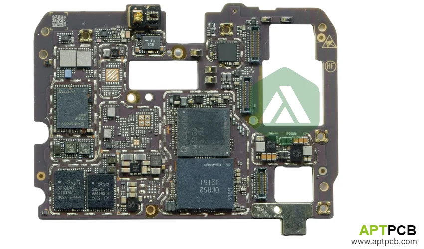
Modern smartphones pack computing power that exceeded supercomputers from two decades ago into a device that fits in your pocket. The PCB at the heart of this achievement represents one of the most demanding applications in electronics manufacturing—combining HDI technology, flex-rigid construction, RF performance, and thermal management within thickness constraints often below 1.0mm for the main logic board.
This guide examines the PCB-level decisions that determine smartphone performance, reliability, and manufacturability: stackup architecture for any-layer HDI, flex-rigid integration for space optimization, RF considerations for 5G and WiFi, thermal solutions within severe space constraints, and the manufacturing capabilities required for high-volume production with sub-50μm features.
In This Guide
- HDI Stackup Architecture for Maximum Component Density
- Flex-Rigid Integration: Connecting Multiple Board Sections
- RF and Antenna PCB Considerations for 5G and WiFi
- Thermal Management Within Ultra-Thin Form Factors
- Manufacturing Requirements for Smartphone PCB Production
- Quality and Reliability Standards for Mobile Devices
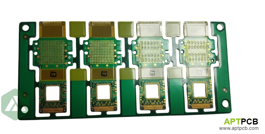
HDI Stackup Architecture for Maximum Component Density
Smartphone main logic boards require component densities exceeding 50 components per square centimeter, with BGA packages featuring pitch as fine as 0.3mm and passive components at 01005 (0.4mm × 0.2mm) size. Achieving this density while maintaining signal integrity and power delivery demands HDI technology with any-layer microvia structures that enable routing escape from ultra-fine-pitch devices.
Any-layer HDI stackups typically employ 8-12 layers with stacked or staggered microvias connecting every layer pair. A typical flagship smartphone might use 10-layer any-layer construction: sequential lamination builds each layer pair with laser-drilled microvias (typically 75-100μm diameter), filled and planarized before the next buildup cycle. This approach eliminates through-hole constraints, allowing designers to place vias anywhere needed for optimal routing.
Stackup Design Considerations
- Layer Count Selection: Entry-level smartphones may use 6-8 layer HDI (1+4+1 or 2+4+2 structures); flagship devices require 10-12 layer any-layer HDI for processor and memory routing complexity.
- Microvia Diameter: Standard 100μm laser vias suffice for 0.4mm pitch BGAs; 0.3mm pitch requires 75μm or smaller vias with corresponding pad size reductions.
- Dielectric Thickness: Ultra-thin prepregs (50-75μm) between signal and reference layers maintain impedance control while minimizing total thickness; core materials at 100-200μm provide structural stability.
- Copper Weights: Outer layers typically use 1/3oz (12μm) or 1/2oz (18μm) base copper; inner layers may use thinner foil (9μm) to enable finer lines after plating.
- Line/Space Capability: Any-layer HDI requires 30/30μm or finer line/space for dense BGA fanout; advanced processes achieve 25/25μm or below.
- Via Fill Requirements: Stacked microvia construction demands complete via fill with conductive or non-conductive paste, plus planarization to ±10μm flatness for reliable layer-to-layer registration.
Designers selecting HDI complexity should balance routing requirements against cost—any-layer HDI costs 3-5× more than standard multilayer and requires longer lead times due to multiple lamination cycles. Advanced PCB manufacturing capabilities directly determine achievable feature sizes and layer counts.
Flex-Rigid Integration: Connecting Multiple Board Sections
Smartphone architectures increasingly employ flex-rigid PCB construction to eliminate connectors, reduce thickness, and enable 3D packaging where rigid sections fold or stack within the device enclosure. A typical implementation might include main logic board, display interface, camera modules, and battery management on separate rigid sections connected by flexible polyimide circuits.
The flex sections replace traditional FPC connectors, eliminating connector height (typically 0.5-1.0mm), reducing assembly complexity, and improving reliability by eliminating connector contact points. However, flex-rigid construction adds manufacturing complexity and cost—expect 2-3× premium over equivalent separate boards with connectors.
Flex-Rigid Architecture Decisions
- Flex Layer Count: Single-layer flex suffices for simple signal routing; high-speed interfaces (MIPI DSI for displays, CSI for cameras) may require dual-layer flex with ground reference.
- Bend Radius Constraints: Dynamic flex areas (hinge applications) require 10× material thickness minimum bend radius; static flex (fold once during assembly) tolerates 6× or tighter.
- Rigid-Flex Transition: The junction between rigid and flex sections represents a reliability vulnerability; proper design includes anchor copper extending into rigid areas and controlled adhesive coverage.
- Polyimide Selection: Standard polyimide (25μm or 50μm) for most applications; thinner polyimide (12.5μm) where ultimate flexibility required; adhesive-less constructions for highest reliability.
- Coverlay Design: Polyimide coverlay protects flex circuits; openings for component mounting require 150-200μm annular ring around pads.
- Stiffener Application: FR-4 or polyimide stiffeners on flex sections provide component mounting support where needed; thickness selection balances rigidity against bend requirements.
Modern flex-rigid PCB construction enables smartphone designs impossible with traditional board-to-board connectors. The technology proves essential for foldable smartphones where the flex section must withstand >200,000 bend cycles.
RF and Antenna PCB Considerations for 5G and WiFi
Smartphone PCBs must support multiple simultaneous radio systems: cellular (4G/5G across multiple bands), WiFi (2.4GHz, 5GHz, and increasingly 6GHz), Bluetooth, GPS, NFC, and potentially UWB. Each system imposes specific PCB requirements for antenna feed, matching networks, and isolation from digital noise sources.
5G introduces particular challenges—sub-6GHz bands extend existing cellular requirements, but mmWave (24-39GHz) demands PCB materials and structures fundamentally different from traditional smartphone designs. mmWave antenna arrays integrate directly onto the PCB or into antenna-in-package modules, requiring low-loss substrates and precise impedance control at frequencies where standard FR-4 exhibits excessive loss.
RF PCB Implementation
- Material Hybrid Approach: Main logic board uses standard high-speed FR-4 (Dk ~3.3-3.5, Df <0.008); RF front-end sections may use modified epoxy or low-loss materials (Df <0.004) for antenna feeds and matching networks.
- mmWave Substrate: 5G mmWave antenna modules require specialized low-loss materials—PTFE-based or LCP (liquid crystal polymer) substrates with Df <0.002 at 28GHz.
- Antenna Integration: Laser-direct-structuring (LDS) antennas on plastic housings connect to main PCB via spring contacts or flex; PCB-integrated antennas use top-layer copper with specific ground clearances.
- Shielding Requirements: RF sections require comprehensive shielding—board-level shield cans, internal ground isolation, and via fencing to prevent coupling between RF and digital sections.
- Impedance Control: RF traces require ±5% impedance tolerance; 50Ω microstrip or grounded coplanar waveguide depending on routing constraints and frequency.
- ESD Protection: All antenna feeds require ESD protection; protection device placement at connector/pad interface with minimal trace length to antenna.
Understanding high-frequency PCB design principles proves essential for smartphone RF performance. The interaction between PCB layout and antenna performance directly affects cellular reception, WiFi range, and battery life through transmit power requirements.
Thermal Management Within Ultra-Thin Form Factors
Modern smartphone processors dissipate 5-10W during peak performance, yet typical smartphone thickness (7-9mm) provides minimal volume for heat spreading. PCB thermal design focuses on extracting heat from processor packages and spreading it across the maximum available area—typically the display assembly and metal frame act as the primary heat sink.
The PCB itself serves as a critical heat spreading medium. Thermal vias directly beneath processor packages conduct heat to internal copper planes, which spread heat laterally to frame contact points. Thermal interface materials (TIMs) bridge gaps between PCB, graphite spreaders, and device housing components.
Thermal Design Approaches
- Thermal Via Arrays: Dense via arrays (0.3mm pitch, 0.2mm drill) beneath high-power components provide vertical heat conduction; filled and capped vias prevent solder wicking during assembly.
- Copper Pour Optimization: Maximum copper coverage on inner layers beneath and around processors; 2oz copper on dedicated thermal layers where stackup permits.
- Graphite Sheet Integration: Synthetic graphite sheets (25-100μm thick, >1000 W/m·K in-plane) spread heat laterally; mounted on PCB back surface with thermal interface materials.
- Vapor Chamber Compatibility: Some designs incorporate vapor chambers; PCB must provide flat, thermally-conductive interface area matching chamber contact region.
- TIM Selection: Gap-filling TIMs (thermal pads or dispensed compounds) bridge PCB-to-housing gaps; thermal conductivity 1-6 W/m·K depending on gap thickness and performance requirements.
- Component Placement Strategy: High-power components spread across board area rather than concentrated; thermal simulation guides placement to prevent hot spots.
Thermal management PCB design in smartphones requires close collaboration between PCB designers, mechanical engineers, and thermal analysts. The extreme space constraints make simulation-guided optimization essential—physical prototypes alone cannot explore the design space efficiently.
RF and Antenna PCB Considerations for 5G and WiFi
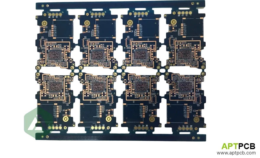
Manufacturing Requirements for Smartphone PCB Production
Smartphone PCB manufacturing combines the most demanding aspects of HDI fabrication with automotive-level quality requirements and consumer electronics volume expectations. Production facilities must achieve <50μm feature resolution consistently across millions of units while maintaining yields above 95% for complex any-layer constructions.
The process complexity for any-layer HDI requires multiple sequential lamination cycles—a 10-layer any-layer board might require 4-5 lamination cycles, each followed by drilling, plating, and imaging. Each cycle introduces registration challenges; cumulative accuracy must maintain layer-to-layer alignment within ±25μm for fine-pitch BGA reliability.
Manufacturing Capability Requirements
- Laser Drilling: UV or CO2 lasers for microvia formation; UV preferred for <75μm vias with controlled depth accuracy; blind via depth control within ±10μm.
- Direct Imaging: LDI (laser direct imaging) required for fine line resolution; traditional photolithography cannot achieve 25/25μm features consistently.
- Via Fill Process: Conductive or non-conductive via fill with planarization; surface flatness ±10μm for reliable subsequent layer buildup.
- Registration Accuracy: Sequential lamination requires X-ray or optical registration systems; layer-to-layer alignment ±25μm or better for stacked via reliability.
- Plating Uniformity: Copper plating thickness uniformity ±10% across panel; critical for impedance control and via fill reliability.
- Inspection Systems: AOI with sub-25μm defect detection; X-ray inspection for via fill and internal layer alignment verification.
Volume smartphone PCB production typically requires mass production capabilities exceeding 100K units monthly per product, with yield and quality metrics under statistical process control.
Quality and Reliability Standards for Mobile Devices
Smartphone PCBs face demanding reliability requirements—devices must survive 2-3 years of daily use across temperature extremes (-20°C to +60°C ambient, with processor operation potentially reaching 100°C), mechanical shock from drops, and humidity exposure. Quality systems must detect defects that could cause field failures while maintaining production throughput.
Major smartphone manufacturers impose qualification requirements beyond standard IPC specifications. Typical requirements include thermal cycling (-40°C to +125°C, 1000 cycles minimum), drop testing (1.5m onto concrete), humidity exposure (85°C/85%RH, 1000 hours), and bend testing for flex-rigid constructions.
Quality and Reliability Framework
- IPC Class 3 Compliance: Smartphone PCBs typically require IPC-6013 Class 3 for flex-rigid, IPC-6012 Class 3 for rigid sections—the highest reliability class for commercial electronics.
- Microsection Analysis: Cross-section inspection of via structures, copper plating, and layer registration; performed on production samples and 100% on qualification lots.
- Electrical Testing: 100% netlist testing via flying probe or fixture; impedance testing on controlled traces; high-voltage isolation testing between power and ground.
- Thermal Cycling: Qualification testing includes -40°C to +125°C cycling; production lots may receive abbreviated cycling as ongoing reliability monitoring.
- HALT/HASS: Highly accelerated life testing during development; highly accelerated stress screening during production for some critical programs.
- Traceability: Full lot traceability from raw materials through finished goods; essential for failure analysis and recall management.
Comprehensive PCB quality systems with documented processes, statistical controls, and continuous improvement programs are table stakes for smartphone PCB suppliers. Major OEMs audit supplier facilities extensively before qualification.
Technical Summary
Smartphone PCB design represents the intersection of multiple advanced technologies: HDI for component density, flex-rigid for space optimization, RF engineering for wireless performance, and thermal management within severe constraints. Success requires expertise across all domains plus manufacturing capabilities that can execute complex designs at consumer electronics volumes.
Key decisions for smartphone PCB projects include stackup complexity (HDI level selection based on component requirements), flex-rigid architecture (balancing integration benefits against cost), RF material selection (loss versus cost trade-offs), and thermal strategy (PCB's role in system thermal solution).
For teams developing smartphone or other compact mobile devices, the PCB partner selection proves critical—capability gaps in HDI processing, flex-rigid fabrication, or quality systems can derail projects regardless of design quality. Start with manufacturing capability verification, then design to demonstrated process capabilities rather than hoping suppliers can stretch beyond their proven limits.