Thermal management determines LED product lifetime, brightness consistency, and color stability more than any other design factor. Systematic thermal design—analyzing heat paths, calculating junction temperatures, selecting appropriate substrates, and validating performance—ensures LED products achieve their reliability potential rather than failing prematurely due to thermal stress.
Many LED thermal failures trace to incomplete design processes: assumptions replacing analysis, rule-of-thumb substrate selection without thermal budget verification, or prototype success misleading designers about production margin. A structured thermal design process prevents these failures by establishing clear requirements and verifying designs meet them.
This guide presents a systematic approach to LED PCB thermal management from initial analysis through production validation.
Analyzing the LED Thermal Path
Thermal path analysis identifies every element heat must traverse from LED junction to ambient, establishing the framework for subsequent thermal design. Each path element contributes thermal resistance that accumulates toward junction temperature.
Understanding path elements enables targeted design improvement where it matters most. Often one element dominates total resistance—improving that element yields significant benefit while optimizing low-resistance elements provides marginal return.
Thermal Path Elements
- LED Package (Rth j-sp): Junction-to-solder-point thermal resistance, specified on LED datasheet. Typically 3-20°C/W depending on package. Fixed by LED selection; design cannot improve.
- Solder Interface: Thermal interface between LED package and PCB copper. Well-formed joints contribute 0.1-0.3°C/W; excessive voiding can increase significantly. Design and assembly process control can optimize.
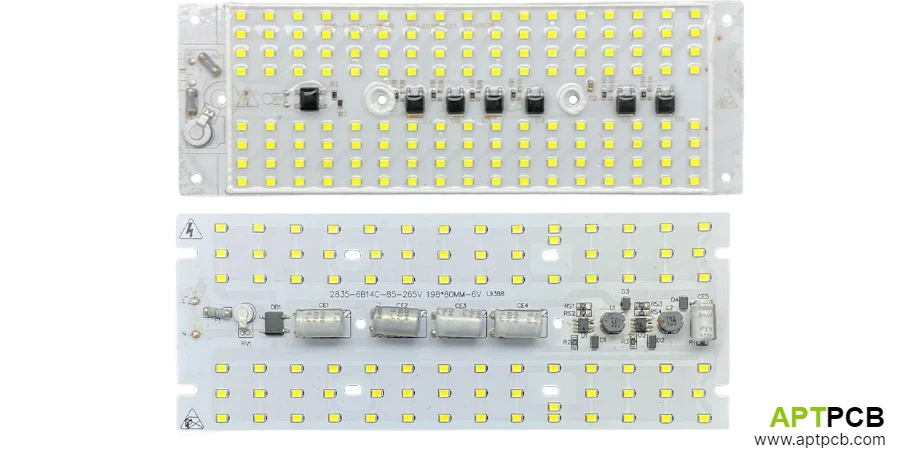
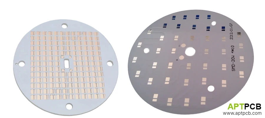
- PCB Substrate: Heat conduction through PCB from LED mounting to heatsink interface. Varies widely (0.3-3°C·cm²/W) depending on substrate technology—major design variable.
- Thermal Interface Material: Connection between PCB bottom and heatsink. Typically 0.1-0.5°C/W depending on material selection and contact pressure.
- Heatsink-to-Ambient: Convection and radiation from heatsink to surrounding air. Often largest thermal resistance in system; highly dependent on heatsink design and airflow conditions.
- Path Resistance Measurement: For critical applications, measure actual thermal resistance of fabricated assemblies. Testing validates analysis assumptions and catches manufacturing issues.
Calculating Junction Temperature
Junction temperature calculation applies thermal path analysis to determine LED operating temperature under specified conditions. This calculation guides substrate selection and validates thermal design adequacy before prototype commitment.
The fundamental relationship is straightforward: junction temperature equals ambient temperature plus total temperature rise through thermal path. Temperature rise equals power dissipation times total thermal resistance.
Calculation Methodology
- Power Dissipation: Calculate thermal power = electrical power × (1 - optical efficiency). Conservative efficiency assumptions protect against optimistic predictions.
- Total Thermal Resistance: Sum resistance contributions from all path elements. Express substrate resistance normalized to area (°C·cm²/W) then convert based on actual thermal contact area.
- Junction Temperature: Tj = T_ambient + (P_thermal × R_th_total). Compare result to target junction temperature with margin for manufacturing variation.
- Worked Example: 10W LED array, 40% efficiency → 6W thermal. Path: LED 10°C/W effective, solder 0.2°C/W, substrate 0.5°C/W, TIM 0.3°C/W, heatsink 1.5°C/W. Total 12.5°C/W. At 6W: 75°C rise. With 45°C ambient: 120°C junction—likely too high.
- Design Iteration: If calculated junction exceeds target, improve thermal path elements. Reduce LED power (derate current), improve substrate, enhance heatsink, or add active cooling.
- Margin Requirement: Maintain 10-15°C margin between calculated junction and LED maximum rating to accommodate manufacturing variation, aging effects, and analysis uncertainty.
Selecting Substrate Based on Requirements
Substrate selection translates thermal analysis into material specification. The analysis establishes required substrate thermal resistance; selection identifies materials meeting that requirement at appropriate cost.
Substrate Selection Process
- Calculate Required Substrate Performance: From thermal budget, determine maximum acceptable substrate thermal resistance. Express as °C·cm²/W to enable material comparison.
- Match to Available Materials: Compare requirement against material capabilities: FR-4 with vias (
2°C·cm²/W achievable), standard MCPCB (1°C·cm²/W), enhanced MCPCB (0.5°C·cm²/W), ceramic substrates (0.03°C·cm²/W). - Consider Cost Trade-offs: Select lowest-cost option meeting requirements. Over-specification wastes cost; under-specification creates reliability problems. Enhanced MCPCB costs ~50% more than standard—justify upgrade through analysis.
- Verify Manufacturability: Confirm selected substrate compatible with intended fabrication processes and supplier capabilities. Exotic substrates may limit sourcing options.
- Document Selection Rationale: Record thermal analysis supporting substrate selection. Documentation enables design review and simplifies future revisions.
- Plan Validation: Define how thermal performance will be verified. Simulation during design, measurement during prototype validation.
Designing Thermal Via Arrays
Thermal vias enhance FR-4 thermal performance by providing parallel heat paths through the substrate. Proper via design significantly improves FR-4 thermal capability, potentially enabling FR-4 use in applications that might otherwise require MCPCB.
Thermal Via Design Guidelines
- Via Placement: Position vias directly under LED thermal pads where heat enters the substrate. Vias outside thermal pad area contribute marginally to heat transfer.
- Via Diameter: Larger vias conduct more heat. 0.3mm minimum; 0.4-0.5mm preferred where space permits. Balance via size against routing constraints.
- Via Pitch: Denser via arrays provide more parallel thermal paths. 0.6-0.8mm pitch typical; verify drilling capability supports specified pitch.
- Via Fill Requirements: Via-in-pad designs require filled and capped vias preventing solder wicking. Specify conductive fill for best thermal performance; non-conductive acceptable where cost constrains.
- Bottom Side Copper: Connect via array to large copper pour on bottom side for heat spreading. Ensure pour extends well beyond via array footprint.
- Thermal Resistance Estimation: Well-designed via array can reduce FR-4 effective thermal resistance by 50-70%. Individual 0.3mm via contributes approximately 0.15 W/°C thermal conductance.
Validating Thermal Performance
Validation confirms actual thermal performance meets design predictions before production commitment. Thermal validation catches analysis errors, manufacturing issues, and assembly problems that would otherwise create field failures.
Validation Methods
- Thermocouple Measurement: Attach thermocouples to LED case, board surface, and heatsink. Measure at thermal equilibrium under specified operating conditions. Calculate junction from case temperature plus LED Rth.
- Infrared Thermal Imaging: Provides visual temperature distribution across assembly. Identifies hot spots, uneven spreading, or interface problems. Useful for troubleshooting thermal issues.
- Forward Voltage Method: LED Vf changes with temperature (approximately -2mV/°C). Measure Vf shift from calibrated reference to infer junction temperature without direct thermal measurement.
- Test Conditions: Validate at worst-case conditions: maximum ambient, maximum power, minimum airflow. Design margin should accommodate variations beyond nominal test conditions.
- Multiple Sample Testing: Test multiple samples to characterize variation. Single sample may not represent production distribution; identify statistical boundaries.
- Pass/Fail Criteria: Establish clear acceptance criteria before testing. Junction temperature below target with specified margin indicates acceptable thermal design.
Summary
Systematic LED PCB thermal management proceeds through analysis, calculation, selection, and validation phases—each building on previous work to ensure reliable thermal performance.
Thermal path analysis identifies contributing elements. Junction temperature calculation predicts operating conditions. Substrate selection matches material capability to requirements. Validation confirms actual performance meets predictions.
This structured approach prevents the incomplete thermal design that causes field failures while avoiding over-specification that adds unnecessary cost. Investment in proper thermal engineering pays dividends through reliable products achieving LED technology's longevity potential.