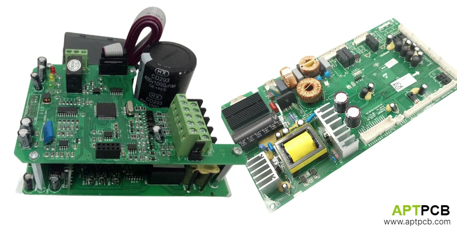
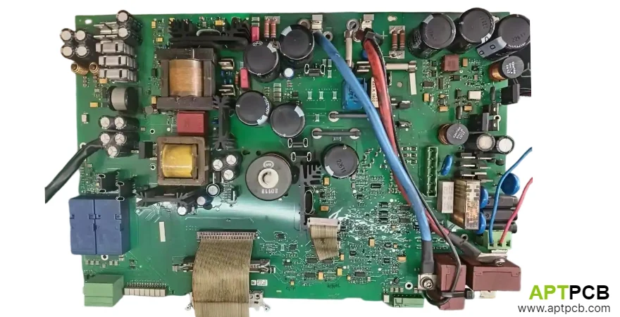
Variable Frequency Drives convert fixed-frequency AC power to variable-frequency, variable-voltage output for precise motor speed control. The PCB must handle kilowatts of power through high-voltage switching stages while maintaining the signal integrity needed for accurate control—all within EMI limits that prevent interference with surrounding equipment.
This guide covers the PCB-level engineering that determines VFD reliability, efficiency, and electromagnetic compatibility in industrial installations.
In This Guide
- Power Stage Layout and Isolation
- Gate Driver Circuit Design
- Current and Voltage Sensing
- EMC Filtering Architecture
- Thermal Management for Power Electronics
- Control Interface Integration
Power Stage Layout and Isolation
VFD power stages switch hundreds of volts at kilohertz frequencies through IGBT or MOSFET bridges. The PCB layout directly affects switching losses, voltage stress, and EMI generation—poor layout can increase losses by 20% or more and create EMI failures that require costly redesign.
Power loop inductance is the critical parameter in high-power switching circuits. Each nanohenry of loop inductance creates voltage spikes during current commutation (V = L × di/dt). With IGBT switching at 5-10kA/μs, even 50nH of parasitic inductance generates 250-500V of overshoot that stresses devices and increases EMI.
The heavy copper PCB construction required for power handling also affects layout options. Thick copper (3-6 oz) changes etching characteristics and minimum feature sizes. Design rules must account for these manufacturing constraints while minimizing loop areas.
Power Stage Layout Principles
- Loop Minimization: DC bus capacitors position directly adjacent to IGBT modules with minimum trace length.
- Laminated Bus Structures: Overlapping copper planes for DC+ and DC- create low-inductance distribution.
- Snubber Integration: RC or RCD snubbers locate at IGBT module terminals, not remotely on the PCB.
- Isolation Barriers: High-voltage power stage separated from control circuits by appropriate creepage distances.
- Thermal Expansion: Heavy copper planes may require attention to CTE mismatch with substrate.
- Current Sharing: Parallel output stages require matched impedance paths for current balance.
Gate Driver Circuit Design
Gate drivers translate control signals into the high-current pulses needed to switch IGBTs rapidly. The driver circuit must provide fast, clean gate drive while maintaining isolation between the control system ground and the high-voltage power stage.
Isolation requirements depend on the power stage topology. In three-phase inverters, high-side drivers reference to phase output nodes that swing across the full DC bus voltage. Isolation must withstand this voltage continuously plus transients from switching events. Gate driver isolators require CMTI (common-mode transient immunity) specifications exceeding 50kV/μs for modern fast-switching designs.
The PCB stackup design for gate driver circuits must maintain signal integrity through the isolation barrier while meeting safety spacing requirements. Gate drive signals carry high-frequency content (fast edges for switching speed) that couples capacitively across isolation barriers—proper layout minimizes this parasitic coupling.
Gate Driver Layout Requirements
- Miller Clamp: Negative gate bias or Miller clamp circuits prevent spurious turn-on from dV/dt coupling.
- Kelvin Source Connection: Separate gate return (Kelvin) from power source reduces inductance effects on gate drive.
- Bootstrap Supply: Bootstrap capacitor sizing and diode selection ensure adequate gate charge through worst-case conditions.
- Propagation Matching: High-side and low-side driver propagation delays match within tens of nanoseconds to prevent shoot-through.
- Isolation Spacing: Creepage and clearance per IEC 60664-1 for working voltage plus transient ratings.
- Gate Resistor Placement: Gate resistors position close to IGBT module for effective damping.
Current and Voltage Sensing
Accurate current and voltage measurements enable vector control algorithms that optimize motor efficiency and dynamic response. The PCB must route these sensitive analog signals through an electrically hostile environment while maintaining measurement accuracy.
Current sensing typically uses Hall-effect sensors or shunt resistors with isolated amplifiers. Shunt-based sensing offers better accuracy and bandwidth but requires isolation amplifiers rated for the common-mode voltage (full DC bus potential plus transients). Hall sensors provide inherent isolation but introduce gain and offset errors that affect control accuracy.
DC bus voltage sensing uses resistive dividers with isolated feedback or dedicated isolated voltage sensors. The sensing circuit must reject the high-frequency content from PWM switching while accurately tracking DC bus variations during regenerative braking or load transients. Analog signal conditioning requires careful attention to filtering and grounding.
Sensing Circuit Design
- Shunt Placement: Current shunts position in DC- leg for single-ended measurement; three shunts enable full three-phase reconstruction.
- Noise Filtering: RC filters on sense signals attenuate switching noise while preserving bandwidth for control loops (typically 1-10kHz corner frequency).
- Differential Routing: Sense signals route as differential pairs with ground reference planes to reject common-mode noise.
- ADC Reference: Stable, low-noise voltage reference for ADC ensures measurement accuracy.
- Sampling Timing: ADC sampling synchronizes with PWM to measure during stable periods, not during switching transitions.
- Calibration Provisions: Test points and calibration coefficients enable production calibration of sense gain and offset.
EMC Filtering Architecture
VFDs generate substantial conducted and radiated emissions from high-power PWM switching. EMC filtering must attenuate these emissions to meet regulatory limits while withstanding the voltage and current stresses of the power circuit. Filter components carry full load current and must survive fault conditions.
Input filtering addresses conducted emissions on the AC mains connection. Common-mode chokes with X and Y capacitors attenuate noise in the 150kHz-30MHz range specified by industrial EMC standards. Filter corner frequency must be low enough for effective attenuation but high enough to avoid resonance issues with input impedance.
Output filtering (dV/dt filters or sine-wave filters) protects motor insulation and reduces motor bearing currents. These filters handle full motor current at PWM switching frequency and must dissipate significant power without overheating. The thermal PCB design must accommodate filter inductor losses.
EMC Filter Implementation
- Common-Mode Choke Sizing: Choke inductance and saturation current rating matched to conducted emission requirements.
- Capacitor Voltage Rating: X and Y capacitors rated for expected transients with appropriate safety approvals.
- Filter Resonance: Damping resistors prevent filter resonance that could amplify specific frequencies.
- Shield Termination: Input cable shields terminate to filter enclosure, not to PCB ground plane.
- Output dV/dt Control: Output chokes or dV/dt filters limit motor terminal voltage rise rate to <500V/μs for cable lengths >10m.
- Grounding Architecture: Single-point ground reference for control circuits; separate high-current power returns.
Thermal Management for Power Electronics
VFD power stages dissipate significant heat from switching and conduction losses. A 10kW drive with 97% efficiency still dissipates 300W internally—concentrated in power semiconductors that must remain below junction temperature limits for reliability.
Power semiconductors mount to heatsinks or cold plates through thermal interface materials. The PCB thermal design conducts heat from device packages to mounting surfaces efficiently. Metal core PCB substrates enable direct mounting of bare-die or thermally-enhanced packages with thermal resistance below 0.5°C/W.
Gate driver circuits also require thermal consideration. Driver ICs dissipate power proportional to gate charge and switching frequency—a driver running IGBTs at 10kHz may dissipate 1-2W. This power must transfer to ambient through the PCB or dedicated thermal paths.
Thermal Design Approaches
- Semiconductor Mounting: Direct mounting to heatsink through thermal interface material; PCB acts as signal carrier only.
- Thermal Via Arrays: Where PCB conducts heat, via arrays under devices reduce thermal resistance to internal planes.
- Copper Weight Selection: 3-6 oz copper in power sections for current capacity and thermal spreading.
- Airflow Coordination: Component placement considers airflow patterns when forced-air cooling is used.
- Temperature Monitoring: NTC sensors on heatsink and in power semiconductors enable thermal protection.
- Derating Guidelines: Thermal design verified at maximum ambient temperature with safety margin for aging.
Control Interface Integration
VFD control systems interface with automation networks, operator controls, and safety systems. The PCB must support these communication interfaces while maintaining isolation from the high-voltage power stage and immunity from the EMI that power switching generates.
Industrial communication protocols (PROFINET, EtherCAT, Modbus TCP) require isolated Ethernet interfaces with industrial-grade transceivers. Serial interfaces for older protocols need RS-485 transceivers with industrial surge protection. The industrial control PCB design practices ensure reliable communication in factory environments.
Digital I/O for start/stop, speed reference, and status signals typically requires 24VDC compatibility with isolation from internal logic levels. Analog inputs accept 0-10V or 4-20mA signals for speed reference—these low-level analog signals are particularly vulnerable to noise pickup from adjacent power circuits.
Control Interface Design
- Ethernet Isolation: 1500Vrms minimum isolation; transformer placement and ground splits per PHY requirements.
- Analog Input Protection: ESD and overvoltage protection on analog inputs; filtering for noise rejection.
- Digital I/O Isolation: Optocoupler or digital isolator interface between field I/O and internal logic.
- Safe Torque Off: Dedicated safety inputs with appropriate isolation and monitoring for STO function.
- Encoder Interface: Differential encoder inputs with termination and filtering for noise immunity.
- Communication Grounding: Network ground referenced to chassis, not to control PCB ground plane.
Summary
VFD PCB design combines power electronics, gate driver engineering, precision sensing, and EMC management into a system that must operate reliably in demanding industrial environments. The high voltages, fast switching edges, and substantial power dissipation create design challenges that require coordinated attention across electrical, thermal, and mechanical domains. Success depends on understanding the interactions between power stage layout, gate drive integrity, sensing accuracy, and EMC performance.