True wireless stereo (TWS) earbuds represent extreme miniaturization—complete audio systems including Bluetooth radio, audio codec, amplifier, battery management, and increasingly active noise cancellation packed into volumes under 5cm³ per earbud. The PCB design must achieve functionality within severe space constraints while meeting audio quality expectations, battery life targets, and comfort requirements that limit weight.
This guide examines the PCB challenges unique to TWS earbuds: ultra-miniature board construction techniques, Bluetooth LE Audio implementation within tiny antennas, battery management for coin cells, audio component integration, and manufacturing processes that maintain quality at the precision required for wearable electronics.
In This Guide
- Ultra-Miniature PCB Construction for Earbuds
- Bluetooth LE Audio and Antenna Design
- Battery Management for Coin Cell Power
- Audio Path Implementation in Minimal Space
- Sensor Integration: ANC and Touch Controls
- Precision Manufacturing for Wearable Electronics
Ultra-Miniature PCB Construction for Earbuds
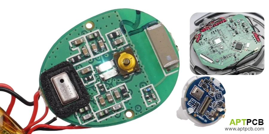
TWS earbud PCBs typically measure under 15mm × 10mm with irregular shapes conforming to ear anatomy. This extreme miniaturization requires high-density interconnect (HDI) technology, via-in-pad construction, and often 0201 or 01005 passive components to achieve necessary functionality.
The small board area limits copper coverage for heat spreading and current carrying—critical considerations given that Bluetooth transmission, audio amplification, and charging all generate heat that the tiny enclosure cannot easily dissipate.
HDI Construction Requirements
- Layer Structure: 3-4 layer HDI typical for TWS; microvia stacks enable component fanout from fine-pitch ICs; 1+2+1 or 2+2+2 structures common.
- Via-in-Pad Design: Component land patterns include filled and capped vias for escape routing; flat surface essential for 0201 and smaller components.
- Line/Space Capability: Dense routing requires 50/50μm or finer; 40/40μm for most challenging designs approaching smartphone density.
- Board Thickness: 0.4-0.6mm total thickness enables stacking with battery; thinner boards require careful handling during assembly.
- Component Miniaturization: 0201 passives standard; 01005 for densest areas; WLCSP packages for ICs minimize height and footprint.
- Irregular Outlines: Custom shapes maximize area within enclosure; tab routing or laser depaneling maintains edge quality for tight enclosure fit.
Achieving required density often requires HDI PCB manufacturing with advanced microvia and fine-line capabilities.
Bluetooth LE Audio and Antenna Design
Bluetooth antenna performance directly affects connection reliability, range, and battery life. The challenge is achieving adequate performance when the entire device measures under 5cm³, with much space occupied by battery, driver, and electronics.
Body loading from the ear significantly affects antenna performance—tuning must account for actual operating environment rather than free-space conditions. The small ground plane available on miniature PCBs further complicates antenna matching.
Layout and impedance control follow the same principles used in high-frequency PCB design.
Antenna Implementation Strategies
- Antenna Options: Chip antennas offer compact size but lower efficiency; PCB-printed antennas need ground clearance; LDS antennas on enclosure conform to available space.
- Ground Plane Effects: Small TWS boards provide limited ground reference; antenna designs must account for actual ground dimensions in tuning.
- Body Loading Compensation: Human ear proximity detunes resonance; design for <-10dB return loss with body loading across 2400-2483.5MHz band.
- Placement Optimization: Position antenna away from battery (metal obstruction) and maximize distance from driver metal components.
- Matching Network: Pi-network or L-network matching compensates for manufacturing variation and body effects; use high-Q components for efficiency.
- Diversity Considerations: Premium earbuds may include antenna diversity for improved reception; requires additional RF switching complexity.
Antenna performance requires empirical optimization with body phantom measurements—simulation alone cannot predict body-loaded performance accurately.
Battery Management for Coin Cell Power
TWS earbuds use small lithium polymer cells (30-70mAh) charging via pogo pins from the case. Battery management must handle charging, protection, and fuel gauging within minimal footprint while maximizing efficiency—every milliwatt impacts playback time.
Quiescent current becomes critical with small batteries; a 5μA quiescent drain on a 50mAh battery represents 1% daily self-discharge, significantly affecting shelf life and standby performance.
Battery Circuit Design
- Integrated BMS: Single-chip solutions combine charger, protection, and fuel gauge; select for <1μA quiescent current to preserve standby life.
- Charge Interface: Pogo pin contact resistance affects charge current; design for 50-100mA charge rate accounting for typical 50-100mΩ contact resistance.
- Protection Functions: Overvoltage (4.25V), undervoltage (2.8V), overcurrent, and short-circuit protection mandatory for lithium cell safety.
- Thermal Monitoring: NTC thermistor monitors cell temperature; disable charging below 0°C and above 45°C per lithium cell specifications.
- Fuel Gauge Accuracy: Coulomb counting with 5-10mΩ sense resistor enables state-of-charge estimation; accuracy affects remaining time display reliability.
- Power Path: System-load operation during charging requires power path management; determines battery versus charge input operation.
Efficient battery management extends playback time—critical competitive differentiator addressed through careful multilayer PCB stackup planning.
Audio Path Implementation in Minimal Space
The audio chain from Bluetooth decoder through amplifier to speaker must achieve quality expectations while fitting minimal space with minimal power. Filterless Class-D amplification dominates TWS designs, relying on speaker inductance for output filtering.
Audio quality perception depends on frequency response, distortion, and channel matching between earbuds. Small drivers (5-7mm) limit bass response, making electronic equalization essential.
Audio Circuit Implementation
- DAC Selection: Integrated DACs in Bluetooth SoCs sufficient for most applications; discrete DACs for premium audio targeting audiophile market segment.
- Amplifier Architecture: Filterless Class-D eliminates output inductor and capacitor; requires compatible speaker and relies on cable/speaker inductance for filtering.
- Power Efficiency: Class-D efficiency 85-90% critical for battery life; avoid linear amplifiers despite simpler implementation—efficiency penalty too severe.
- Speaker Matching: Amplifier output impedance and driver impedance must match for maximum power transfer; typical drivers 16-32Ω impedance.
- EQ Implementation: DSP-based equalization compensates for small driver response; typical boost below 200Hz, presence adjustments 2-6kHz.
- Channel Matching: Left/right matching requires consistent component selection and calibration; mismatch creates audible stereo image issues.
Audio performance at miniature scale requires careful component selection and layout—noise coupling easily degrades performance in dense designs.
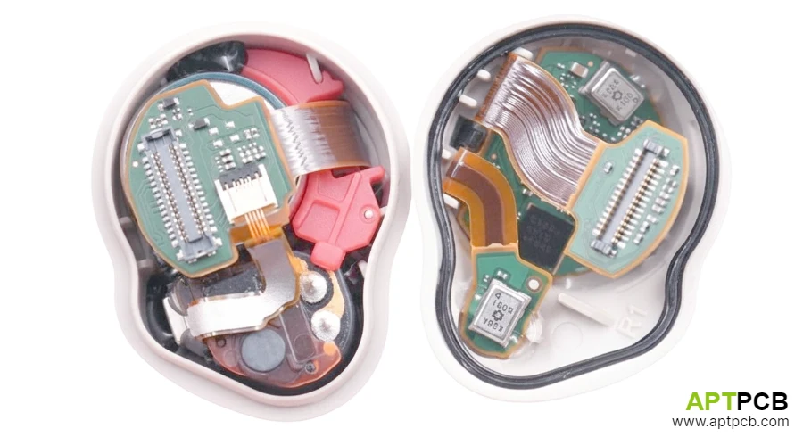
Sensor Integration: ANC and Touch Controls
Premium TWS earbuds include active noise cancellation (ANC) requiring external microphones for ambient sound pickup, internal microphones for error correction, and DSP processing for anti-noise generation. Touch controls add capacitive sensing to the feature set, requiring sensitive analog circuits in close proximity to RF and digital systems.
ANC implementation doubles or triples microphone count compared to basic earbuds—each microphone requires careful acoustic design and electrical routing to achieve noise cancellation performance.
Sensor Implementation
- ANC Microphone Configuration: Feed-forward (external) plus feedback (internal) microphones typical; hybrid ANC using both achieves best performance but adds complexity.
- Microphone Matching: ANC performance requires closely matched microphones; specify tight sensitivity tolerance (±1dB) and phase matching.
- Touch Sensing: Capacitive touch detection on enclosure surface; sensor electrode routing must avoid noise coupling from RF and audio circuits.
- In-Ear Detection: IR proximity sensor or capacitive sensing detects insertion; auto-pause functionality depends on reliable detection.
- Bone Conduction: Premium designs add bone conduction sensor for voice call clarity enhancement; requires mechanical coupling to enclosure.
- Sensor Routing: All sensor signals benefit from ground shielding traces; particularly important for capacitive touch near Bluetooth antenna.
Multiple sensor systems create integration challenges—careful PCB partitioning and ground management prevent interference between subsystems.
Precision Manufacturing for Wearable Electronics
TWS PCB manufacturing combines smartphone-level miniaturization with high-volume consumer electronics economics. The precision required for 0201 placement, microvia formation, and fine-line imaging must be maintained across millions of units while meeting aggressive cost targets.
Assembly challenges include handling tiny boards through pick-and-place, achieving solder paste deposition accuracy for 0201 and smaller components, and functional testing at sufficient throughput for volume production.
Manufacturing Requirements
- Fabrication Precision: ±25μm registration for microvia alignment; ±15μm for fine-line imaging; tight tolerances throughout process chain.
- Solder Paste Control: 3mil stencils for 0201; accurate aperture design prevents insufficient paste or bridging; SPI verification essential.
- Pick-and-Place Accuracy: ±30μm placement accuracy for 0201; vision alignment on fiducials and component features.
- Reflow Profile: Careful profile development for dense assemblies; temperature uniformity across small boards prevents defects.
- AOI Adaptation: Automated optical inspection tuned for miniature components; false call reduction while maintaining defect capture.
- Functional Testing: Audio response, Bluetooth connectivity, and sensor function verification; test fixture design for irregular board shapes.
Volume TWS production requires rigid-flex PCB manufacturing matching or exceeding smartphone assembly precision.
Technical Summary
TWS earbud PCB design pushes miniaturization limits while maintaining audio quality, connectivity performance, and battery life. Success requires HDI construction with fine features, antenna design optimized for body-worn operation, and efficient battery management maximizing limited cell capacity.
Key decisions include construction complexity (HDI level based on component count and package types), antenna approach (chip, PCB, or LDS based on available space and performance requirements), and sensor integration level (basic versus ANC-equipped variants).
Manufacturing partner selection should prioritize demonstrated miniature assembly capability and process control adequate for consistent quality across millions of units.
Looking for a manufacturing-ready earbuds mainboard? See our PCB manufacturing capabilities.