
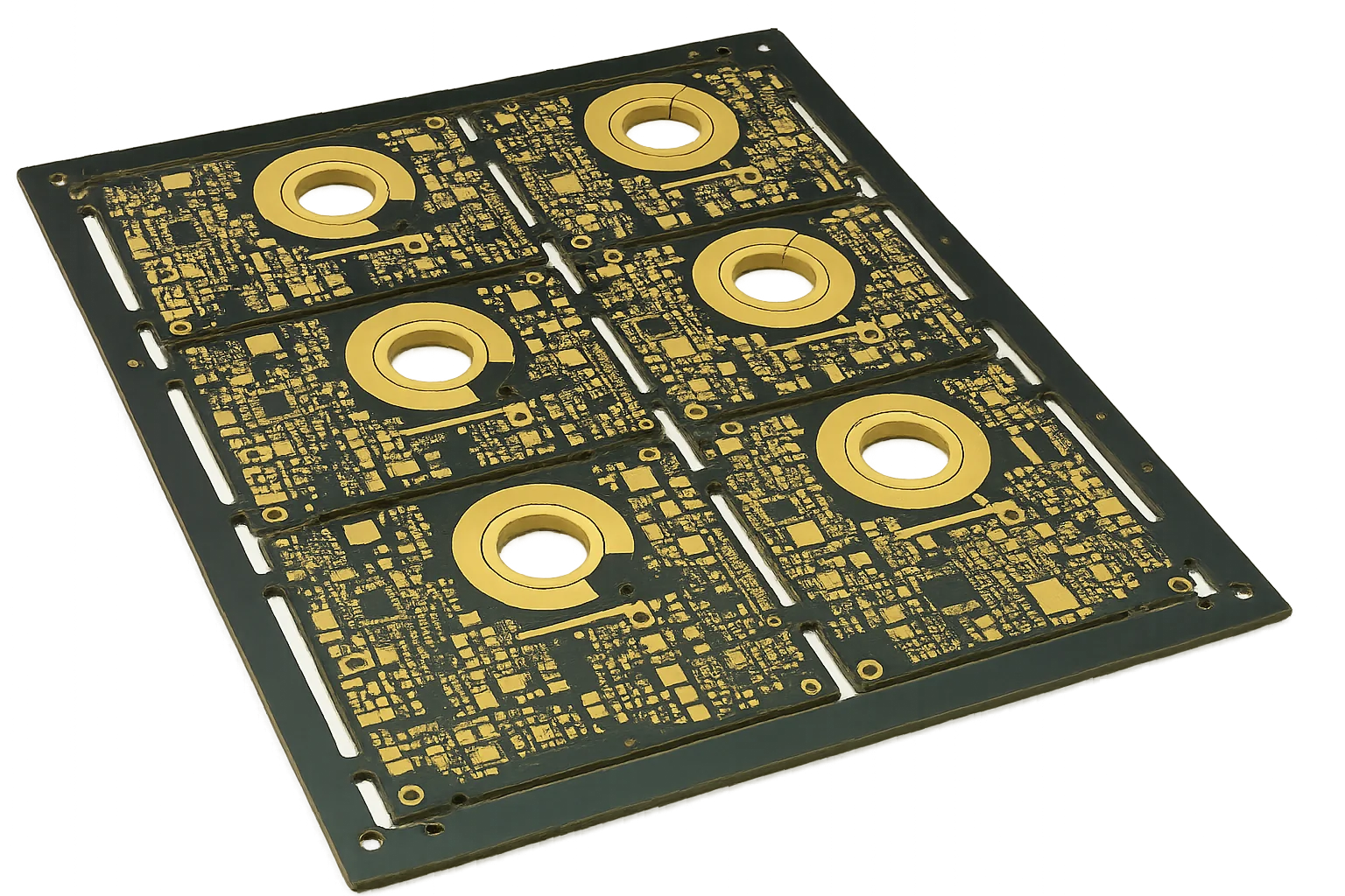
Power electronics, electric vehicle (EV) traction inverters, renewable energy power converters, and high-reliability industrial motor drives increasingly replace bulky mechanical busbars and discrete cable harnesses with heavy copper printed circuit boards ($\ge 3\text{ oz/ft}^2$ or $105\ \mu\text{m}$). Embedding high-current conductors directly into a planar multilayer substrate eliminates bolted terminal contact resistance, reduces enclosure height profiles by up to $50%$, and improves high-vibration reliability in automotive and aerospace environments.
However, designing with thick copper introduces complex physical constraints that standard DFM rules cannot handle. Sizing high-current traces with legacy IPC-2221 charts results in oversized conductors because IPC-2221 relies on 1950s single-conductor air measurements that ignore modern multilayer dielectric thermal conduction and adjacent ground planes. Under IPC-2152, conductor cross-sectional area is balanced against allowable temperature rise ($\Delta T$), copper thickness, board thickness, and adjacent plane thermal sinking. Chemical etch undercut produces trapezoidal conductor profiles requiring aggressive CAM pre-compensation, prepreg resin volumes must satisfy $V_{\text{resin}} \ge 1.30 \times V_{\text{channel}}$ to prevent lamination voiding, and high thermal mass demands multi-stage preheating ($110^\circ\text{C} - 130^\circ\text{C}$) to achieve the $\ge 75%$ through-hole barrel fill mandated by IPC-A-610 Class 3.
| Design Parameter | Standard Copper ($0.5\text{ oz} - 2\text{ oz}$) | Heavy Copper ($3\text{ oz} - 5\text{ oz}$) | Extreme Copper ($6\text{ oz} - 10\text{ oz}+$) | Primary Fabrication Constraint |
|---|---|---|---|---|
| Current Handling Range | $\le 15\text{A}$ continuous | $20\text{A} - 60\text{A}$ continuous | $60\text{A} - 150\text{A}+$ continuous | IPC-2152 thermal rise calculation ($\Delta T$) |
| Minimum Trace / Space (CAD) | $4 / 4\text{ mil}$ ($0.10\text{ mm}$) | $10 / 10\text{ mil}$ ($0.25\text{ mm}$) | $16 / 16\text{ mil} - 25 / 25\text{ mil}$ | Chemical etch factor ($F = T/U$) and lateral undercut |
| Prepreg Lamination Package | Standard 1080 / 2116 / 7628 | High-Resin 1080 HR / 2116 HR | Multi-ply High-Resin Glass Packages | Resin starvation prevention ($V_{\text{resin}} \ge 1.30 V_{\text{channel}}$) |
| Drill Annular Ring Allowance | Standard $+3\text{ mil}$ ($0.075\text{ mm}$) | $+4\text{ mil}$ ($0.10\text{ mm}$) | $+5\text{ mil} - 6\text{ mil}$ ($0.125\text{ mm} - 0.15\text{ mm}$) | High cutting torque and drill bit deflection |
| Assembly Preheating Protocol | Ambient to $90^\circ\text{C}$ bottom-side | $100^\circ\text{C} - 115^\circ\text{C}$ dual-side | $120^\circ\text{C} - 135^\circ\text{C}$ multi-stage | IPC-A-610 Class 3 vertical hole fill ($\ge 75%$) |
For specific factory tolerances, raw material availability, and formal manufacturing release gates, review our dedicated Heavy Copper PCB Manufacturing Capabilities. When power density requires extreme planar thermal conduction exceeding dielectric limits, evaluate Metal Core PCB (MCPCB) Capabilities and standard Rigid PCB Capabilities. For assembly process windows, review Thick Copper Selective Soldering & Assembly.
Table of Contents
- What Defines Heavy Copper vs. Extreme Copper?
- IPC-2152 vs. Legacy IPC-2221: Thermal Conduction Physics
- IPC-2152 Conductor Ampacity & Width Sizing Matrix
- Etch Factor, Lateral Undercut, and CAM Compensation
- Multilayer Lamination & Resin Voiding Mitigation
- Assembly Thermal Mass & IPC-A-610 Class 3 Soldering
- Heavy Copper DFM & RFQ Submission Checklist
- Frequently Asked Questions (FAQ)
What Defines Heavy Copper vs. Extreme Copper?
In standard PCB fabrication, outer layers typically use 1 oz finished copper ($35\ \mu\text{m}$ or $1.4\text{ mil}$) and inner layers use 0.5 oz or 1 oz foil. In power electronics, motor drives, and renewable energy conversion, current demands quickly exceed the thermal capacity of standard foil.
Standard Copper:    0.5 oz to 2 oz  (18 µm to 70 µm)   --> Signal & Low-Power Control
Heavy Copper:       3 oz to 5 oz    (105 µm to 175 µm) --> Power Supplies, Industrial Drives, 20A–60A
Extreme Copper:     6 oz to 20 oz+  (210 µm to 700 µm) --> EV Traction Inverters, Military Radar, 60A–200A+
Integrating heavy copper directly into the PCB delivers four decisive mechanical and electrical advantages over discrete busbars:
- Elimination of Point-of-Contact Interconnect Failures: Discrete copper busbars rely on bolted terminals, crimped lugs, or press-fit pins. Under heavy thermal cycling and high-vibration automotive or aerospace conditions, these mechanical joints loosen, oxidize, and form catastrophic localized hot spots. Heavy copper traces are monolithic, solid-state copper paths.
- Compact Enclosure Profiles: Bulky external wiring harnesses and elevated busbars demand tall mechanical clearances. Planar heavy copper conductors embed within the $1.6\text{ mm}$ to $3.2\text{ mm}$ substrate, cutting power module enclosure volume by up to $50%$.
- Optimized $I^2R$ Power Loss: Distributing current across wide, flat copper planes maximizes surface area for convective and conductive cooling while minimizing high-frequency skin-effect resistance.
- Co-location of Logic and Power: Multilayer heavy copper designs allow fine-pitch microcontroller signal routing on outer layers while dedicating internal 4 oz or 6 oz layers to high-current power buses.
IPC-2152 vs. Legacy IPC-2221: Thermal Conduction Physics
For over two decades, power electronics engineers sized high-current traces using the formulas found in IPC-2221 (formerly IPC-D-275). These legacy formulas calculate conductor cross-sectional area based on:
$$I = k \cdot \Delta T^{0.44} \cdot A^{0.725}$$
Where:
- $k = 0.048$ for external layers and $k = 0.024$ for internal layers
- $\Delta T$ is allowable temperature rise above ambient ($^\circ\text{C}$)
- $A$ is trace cross-sectional area ($\text{mil}^2$)
The Flaw in Legacy IPC-2221
IPC-2221 data was derived in 1954 from single-sided, 1/16-inch phenolic paper-based test boards with a single isolated copper track suspended in still air. In modern multilayer FR-4 or polyimide circuit boards, this thermal model completely breaks down:
- Dielectric Conduction Sinks Heat: FR-4 substrate material has a bulk thermal conductivity of $k \approx 0.30 - 0.45\text{ W/m}\cdot\text{K}$. Thermal energy does not merely radiate from the copper surface into surrounding air; it conducts into the core dielectric.
- Adjacent Plane Heat Spreading: When a heavy copper power trace is routed over an internal ground plane (even a 1 oz or 2 oz plane), the ground plane acts as a lateral heat spreader, dropping trace temperature rise by $30% - 60%$.
- Severe Oversizing: Using IPC-2221 to size an 80A conductor forces designers to lay out massive, unmanufacturable traces that waste valuable real estate.
The IPC-2152 Sizing Method
IPC-2152 (Standard for Determining Current-Carrying Capacity in Printed Board Design) replaced IPC-2221 by establishing empirical thermal curves from modern multilayer test coupons. The standard demonstrates that conductor current-carrying capacity is governed by:
- Copper thickness (weight) and trace width
- Total printed board thickness (a thicker board conducts heat away faster)
- Proximity to adjacent thermal-plane copper
- Substrate material thermal conductivity ($k$)
IPC-2152 Conductor Ampacity & Width Sizing Matrix
The following engineering lookup table provides required conductor widths for continuous direct current (DC) loads across 3 oz, 4 oz, 6 oz, 8 oz, and 10 oz copper weights, based on an ambient temperature of $25^\circ\text{C}$ with a nominal 1.6 mm thick FR-4 board.
| Current Load (Amperes) | Allowable Temp Rise ($\Delta T$) | 3 oz ($105\ \mu\text{m}$) Trace Width | 4 oz ($140\ \mu\text{m}$) Trace Width | 6 oz ($210\ \mu\text{m}$) Trace Width | 8 oz ($280\ \mu\text{m}$) Trace Width | 10 oz ($350\ \mu\text{m}$) Trace Width |
|---|---|---|---|---|---|---|
| 20 A | $\Delta T = 10^\circ\text{C}$ | $4.8\text{ mm}$ ($190\text{ mil}$) | $3.5\text{ mm}$ ($138\text{ mil}$) | $2.2\text{ mm}$ ($87\text{ mil}$) | $1.6\text{ mm}$ ($63\text{ mil}$) | $1.2\text{ mm}$ ($47\text{ mil}$) |
| 20 A | $\Delta T = 20^\circ\text{C}$ | $3.2\text{ mm}$ ($126\text{ mil}$) | $2.3\text{ mm}$ ($91\text{ mil}$) | $1.5\text{ mm}$ ($59\text{ mil}$) | $1.1\text{ mm}$ ($43\text{ mil}$) | $0.85\text{ mm}$ ($33\text{ mil}$) |
| 20 A | $\Delta T = 30^\circ\text{C}$ | $2.5\text{ mm}$ ($98\text{ mil}$) | $1.8\text{ mm}$ ($71\text{ mil}$) | $1.2\text{ mm}$ ($47\text{ mil}$) | $0.85\text{ mm}$ ($33\text{ mil}$) | $0.65\text{ mm}$ ($26\text{ mil}$) |
| 40 A | $\Delta T = 10^\circ\text{C}$ | $12.5\text{ mm}$ ($492\text{ mil}$) | $9.2\text{ mm}$ ($362\text{ mil}$) | $5.8\text{ mm}$ ($228\text{ mil}$) | $4.2\text{ mm}$ ($165\text{ mil}$) | $3.2\text{ mm}$ ($126\text{ mil}$) |
| 40 A | $\Delta T = 20^\circ\text{C}$ | $8.4\text{ mm}$ ($330\text{ mil}$) | $6.1\text{ mm}$ ($240\text{ mil}$) | $3.9\text{ mm}$ ($154\text{ mil}$) | $2.8\text{ mm}$ ($110\text{ mil}$) | $2.1\text{ mm}$ ($83\text{ mil}$) |
| 40 A | $\Delta T = 30^\circ\text{C}$ | $6.6\text{ mm}$ ($260\text{ mil}$) | $4.8\text{ mm}$ ($189\text{ mil}$) | $3.1\text{ mm}$ ($122\text{ mil}$) | $2.2\text{ mm}$ ($87\text{ mil}$) | $1.7\text{ mm}$ ($67\text{ mil}$) |
| 60 A | $\Delta T = 10^\circ\text{C}$ | $21.0\text{ mm}$ ($827\text{ mil}$) | $15.5\text{ mm}$ ($610\text{ mil}$) | $9.8\text{ mm}$ ($386\text{ mil}$) | $7.1\text{ mm}$ ($280\text{ mil}$) | $5.4\text{ mm}$ ($213\text{ mil}$) |
| 60 A | $\Delta T = 20^\circ\text{C}$ | $14.2\text{ mm}$ ($559\text{ mil}$) | $10.4\text{ mm}$ ($409\text{ mil}$) | $6.6\text{ mm}$ ($260\text{ mil}$) | $4.8\text{ mm}$ ($189\text{ mil}$) | $3.6\text{ mm}$ ($142\text{ mil}$) |
| 60 A | $\Delta T = 30^\circ\text{C}$ | $11.2\text{ mm}$ ($441\text{ mil}$) | $8.2\text{ mm}$ ($323\text{ mil}$) | $5.2\text{ mm}$ ($205\text{ mil}$) | $3.7\text{ mm}$ ($146\text{ mil}$) | $2.8\text{ mm}$ ($110\text{ mil}$) |
| 80 A | $\Delta T = 10^\circ\text{C}$ | Not Recommended | $22.5\text{ mm}$ ($886\text{ mil}$) | $14.2\text{ mm}$ ($559\text{ mil}$) | $10.3\text{ mm}$ ($406\text{ mil}$) | $7.8\text{ mm}$ ($307\text{ mil}$) |
| 80 A | $\Delta T = 20^\circ\text{C}$ | $20.8\text{ mm}$ ($819\text{ mil}$) | $15.2\text{ mm}$ ($598\text{ mil}$) | $9.6\text{ mm}$ ($378\text{ mil}$) | $6.9\text{ mm}$ ($272\text{ mil}$) | $5.2\text{ mm}$ ($205\text{ mil}$) |
| 80 A | $\Delta T = 30^\circ\text{C}$ | $16.5\text{ mm}$ ($650\text{ mil}$) | $12.0\text{ mm}$ ($472\text{ mil}$) | $7.6\text{ mm}$ ($299\text{ mil}$) | $5.5\text{ mm}$ ($217\text{ mil}$) | $4.1\text{ mm}$ ($161\text{ mil}$) |
| 100 A | $\Delta T = 20^\circ\text{C}$ | Not Recommended | $20.5\text{ mm}$ ($807\text{ mil}$) | $12.8\text{ mm}$ ($504\text{ mil}$) | $9.2\text{ mm}$ ($362\text{ mil}$) | $7.0\text{ mm}$ ($276\text{ mil}$) |
| 100 A | $\Delta T = 30^\circ\text{C}$ | $22.4\text{ mm}$ ($882\text{ mil}$) | $16.3\text{ mm}$ ($642\text{ mil}$) | $10.2\text{ mm}$ ($402\text{ mil}$) | $7.4\text{ mm}$ ($291\text{ mil}$) | $5.6\text{ mm}$ ($220\text{ mil}$) |
| 120 A | $\Delta T = 30^\circ\text{C}$ | Not Recommended | $21.2\text{ mm}$ ($835\text{ mil}$) | $13.2\text{ mm}$ ($520\text{ mil}$) | $9.5\text{ mm}$ ($374\text{ mil}$) | $7.2\text{ mm}$ ($283\text{ mil}$) |
Note: Sizing assumes external traces with no forced airflow. When internal ground/power planes exist within $0.2\text{ mm}$ ($8\text{ mil}$) of the conductor, trace width can be reduced by $15% - 25%$ due to planar conduction sinking.
Etch Factor, Lateral Undercut, and CAM Compensation
The most formidable manufacturing bottleneck in heavy copper fabrication is the chemical wet-etching process. In standard $1\text{ oz}$ boards ($35\ \mu\text{m}$ thick), the chemical etchant dissolves copper vertically down to the substrate while producing minor lateral undercut. However, when etching through $10\text{ oz}$ copper ($350\ \mu\text{m}$ thick), the etchant attacks the sidewalls of the trace for an extended period, creating a severe trapezoidal cross-section.
                         Photoresist Mask (Width = W_mask)
                               ┌─────────────────┐
                               │                 │
      ┌────────────────────────┴─────────────────┴────────────────────────┐
      │                        Top Width (W_top)                          │
      │                     /───────────────────────\                     │
      │                    /                         \                    │
      │  Lateral          /                           \   Lateral         │
      │  Undercut (U)    /                             \  Undercut (U)    │
      │                 /                               \                 │
      └────────────────/─────────────────────────────────\────────────────┘
                              Base Width (W_base)
      ═════════════════════════════════════════════════════════════════════  Substrate
The Chemical Etch Factor ($F$)
The Etch Factor ($F$) is the ratio of vertical copper thickness ($T$) to the amount of lateral undercut ($U$):
$$F = \frac{T}{U} = \frac{T}{\frac{W_{\text{base}} - W_{\text{top}}}{2}}$$
- Standard chemical etching lines achieve an etch factor of $F \approx 2.0$ to $3.0$ for heavy copper.
- For a $6\text{ oz}$ trace ($T = 210\ \mu\text{m}$), an etch factor of $2.5$ produces a lateral undercut of: $$U = \frac{210\ \mu\text{m}}{2.5} = 84\ \mu\text{m}\ (3.3\text{ mil})\text{ per side}$$
- Consequently, the top of the finished copper trace ($W_{\text{top}}$) will be $168\ \mu\text{m}$ ($6.6\text{ mil}$) narrower than the base of the trace ($W_{\text{base}}$).
CAM Line & Space Compensation Guidelines
To ensure the top of the finished trace meets electrical cross-section requirements without bridging the base into adjacent conductors, CAM engineers must pre-widen traces on the phototool. As a layout designer, you must provide adequate CAD spacing to allow for this mandatory CAM enlargement.
| Base Copper Foil Weight | Nominal Finished Thickness | Minimum Finished Trace Width ($W_{\text{CAD}}$) | Minimum Required Clearance ($S_{\text{CAD}}$) | Required CAM Pre-Compensation (Per Side) |
|---|---|---|---|---|
| 2 oz / ft² | $70\ \mu\text{m}$ ($2.8\text{ mil}$) | $6\text{ mil}$ ($0.15\text{ mm}$) | $6\text{ mil}$ ($0.15\text{ mm}$) | $+1.5\text{ mil}$ ($0.038\text{ mm}$) |
| 3 oz / ft² | $105\ \mu\text{m}$ ($4.1\text{ mil}$) | $8\text{ mil}$ ($0.20\text{ mm}$) | $10\text{ mil}$ ($0.25\text{ mm}$) | $+2.5\text{ mil}$ ($0.063\text{ mm}$) |
| 4 oz / ft² | $140\ \mu\text{m}$ ($5.5\text{ mil}$) | $10\text{ mil}$ ($0.25\text{ mm}$) | $12\text{ mil}$ ($0.30\text{ mm}$) | $+3.5\text{ mil}$ ($0.089\text{ mm}$) |
| 6 oz / ft² | $210\ \mu\text{m}$ ($8.3\text{ mil}$) | $14\text{ mil}$ ($0.35\text{ mm}$) | $16\text{ mil}$ ($0.40\text{ mm}$) | $+5.0\text{ mil}$ ($0.127\text{ mm}$) |
| 8 oz / ft² | $280\ \mu\text{m}$ ($11.0\text{ mil}$) | $18\text{ mil}$ ($0.45\text{ mm}$) | $20\text{ mil}$ ($0.50\text{ mm}$) | $+7.0\text{ mil}$ ($0.178\text{ mm}$) |
| 10 oz / ft² | $350\ \mu\text{m}$ ($13.8\text{ mil}$) | $22\text{ mil}$ ($0.55\text{ mm}$) | $25\text{ mil}$ ($0.63\text{ mm}$) | $+9.0\text{ mil}$ ($0.228\text{ mm}$) |
[!WARNING] If you route $6\text{ oz}$ traces in CAD with standard $8\text{ mil}$ spacing, the CAM engineer cannot apply the mandatory $+5\text{ mil}$ etch compensation. The board cannot be fabricated without triggering an Engineering Query (EQ) that delays production. Always consult the clearance lookup table before locking your power layout.
Multilayer Lamination & Resin Voiding Mitigation
In multilayer heavy copper boards, the trenches between etched copper conductors form deep physical canyons. During high-temperature vacuum lamination, the prepreg bonding sheets must melt, flow, and completely fill these trenches before cross-linking (polymerizing).
                      Prepreg Bonding Layer (Melted Resin Flow)
        ┌─────────────────────────────────────────────────────────────────┐
        │                                                                 │
   ═════╧═══════════                                     ═════════════════╧═════
   [ 6 oz Trace A ] ◄────── Trench to be filled ────────► [ 6 oz Trace B ]
   (Height = 210 µm)       with prepreg resin             (Height = 210 µm)
   ═════════════════                                     ═══════════════════════
   ───────────────────────────────────────────────────────────────────────────── Core Substrate
The Physics of Resin Starvation
If the volume of resin supplied by the prepreg is lower than the volume of empty copper trenches, the lamination press enters a state of resin starvation:
- Dielectric Micro-Voids: Trapped air and volatile gas pockets form along the sidewalls of thick conductors. Under high working voltages ($>400\text{V}$ in EV battery systems), these voids trigger localized Partial Discharge (PD), which erodes the dielectric and causes catastrophic dielectric breakdown.
- Measling and Delamination: Under subsequent reflow soldering ($240^\circ\text{C} - 260^\circ\text{C}$), moisture trapped within these voids vaporizes, generating explosive steam pressure that tears inner layers apart.
Lamination Balance & Prepreg Selection Rules
To guarantee void-free lamination, the available prepreg resin volume ($V_{\text{resin}}$) must satisfy the following safety factor relative to the channel volume ($V_{\text{channel}}$):
$$V_{\text{resin}} \ge 1.30 \times V_{\text{channel}}$$
- High-Resin (HR) Prepregs: Standard prepregs (such as 7628 with $43%$ resin content) cannot provide sufficient liquid resin. APTPCB uses specialized high-resin glass fabrics, including:
- 1080 HR ($68% - 75%$ resin content)
- 2116 HR ($58% - 64%$ resin content)
- Multi-Ply Prepreg Stacks: Never use a single thick sheet of prepreg to bridge a $4\text{ oz}$ to $10\text{ oz}$ copper gap. APTPCB deploys a multi-ply stacking strategy: a high-flow 1080 HR sheet is placed directly against the copper to fill the trenches, backed by a structural 2116 or 7628 glass sheet to establish precise dielectric spacing.
- Thieving (Copper Balancing): Large, unrouted empty areas on inner layers must be filled with non-functional copper hatching ("copper thieving"). Copper thieving equalizes the channel volume across the production panel, preventing localized resin sinkholes.
Panel Warpage (Bow & Twist) Control
Heavy copper generates massive mechanical tensile stress during thermal cool-down. Under IPC-6012 Section 3.4.4, finished rigid boards must maintain a bow and twist of less than $0.75%$ (or $0.50%$ for automated SMT lines).
- Stackup Symmetry Rule: Copper weight must be balanced symmetrically about the center core. A 4-layer board with 6 oz on Layer 2 and 1 oz on Layer 3 will warp into a potato chip during reflow. Layer 2 and Layer 3 must have matched copper weights and matched dielectric distances to outer layers.
Assembly Thermal Mass & IPC-A-610 Class 3 Soldering
Designing a buildable bare heavy copper board is only half the engineering challenge. When the bare board arrives at the surface-mount (SMT) and through-hole (THT) assembly line, the massive volume of copper acts as an enormous heat sink that rapidly draws thermal energy away from soldering irons and solder wave nozzles.
Solder Starvation in Heavy Copper Barrels
According to IPC-A-610 Class 3 (High-Performance Electronic Products), through-hole solder connections must achieve a minimum of $75%$ vertical hole fill (barrel fill):
[ Component Lead ]          │   │
[ Top Solder Fillet ]   ────┴───┴────  ◄── Top Side Fillet Required (Class 3)
[ Plated Barrel ]      │▒▒▒▒│   │▒▒▒▒│
                       │▒▒▒▒│   │▒▒▒▒│ ◄── Minimum 75% Vertical Fill
                       │▒▒▒▒│   │▒▒▒▒│     (Zero voids permitted in Class 3)
[ Bottom Solder Source] ────┬───┬────
                            │   │
If a power connector pin connects directly to a solid $6\text{ oz}$ inner ground plane without thermal isolation, the plane sinks heat faster than a standard wave or hand-soldering iron can deliver it. The solder freezes prematurely inside the barrel, yielding cold solder joints and failing Class 3 inspection with less than $40%$ vertical fill.
Assembly Thermal Relief Design Rules
- Direct Tie vs. Thermal Relief:
- For manual hand soldering, thermal relief cutouts are mandatory. Spoke width must be expanded to $25\text{ mil} - 40\text{ mil}$ ($0.63\text{ mm} - 1.0\text{ mm}$) to support high current while preventing soldering iron freeze.
- For automated selective soldering, solid $360^\circ$ direct ties can be used only if the assembly facility employs preheating protocols.
- Selective Soldering Multi-Stage Preheating Protocol:
- Standard assemblies enter selective soldering with bottom-side preheat temperatures around $90^\circ\text{C} - 100^\circ\text{C}$.
- Heavy copper boards ($\ge 4\text{ oz}$) require multi-stage bottom and top-side infrared/convection preheating up to $120^\circ\text{C} - 135^\circ\text{C}$ before flux and solder nozzle contact.
- Solder nozzle contact dwell time must be increased from the standard $1.5\text{ seconds}$ up to $3.5 - 5.0\text{ seconds}$ using nitrogen-inerted mini-wave nozzles ($285^\circ\text{C} - 300^\circ\text{C}$ pot temperature) to guarantee full capillary wetting up through the barrel.
- Solder Mask Thickness Over Heavy Copper Edges:
- Liquid Photoimageable (LPI) solder mask applied by standard curtain coating pulls thin across the sharp $90^\circ$ top corners of thick copper traces. On $4\text{ oz}$ to $10\text{ oz}$ traces, edge coverage can drop below $0.2\text{ mil}\ (5\ \mu\text{m})$, risking dielectric pinhole flashover.
- APTPCB mandates dual-pass electrostatic spray coating or vacuum dry film solder mask to guarantee a minimum of $0.8\text{ mil}\ (20\ \mu\text{m})$ mask coverage over all sharp conductor corners.
Manufacturing & CAM Release Guidelines
To obtain an accurate manufacturing review and buildable quote without engineering holds, ensure your procurement and design data package conforms to these core release criteria:
| Engineering Gate | Standard Specification | High-Reliability Power Rule |
|---|---|---|
| Copper Weight Declaration | Distinguish between base copper foil weight and finished plated copper thickness | Specify finished thickness on drawing notes (e.g., "Layer 2 finished copper: 6.0 oz / 210 µm") |
| CAM Spacing Allowances | Adhere to minimum trace spacing table in Section 4 | Maintain minimum clearances: $10\text{ mil}$ for 3 oz; $16\text{ mil}$ for 6 oz; $25\text{ mil}$ for 10 oz |
| Layer Copper Symmetry | Match copper distribution across opposing core sides | Copper area delta between paired layers must not exceed $\pm 15%$ to prevent bow and twist |
| Drill-to-Copper Spacing | Provide adequate clearance for heavy copper drill deflection | Inner layer drill-to-copper clearance $\ge 18\text{ mil}$ ($0.45\text{ mm}$) for $\le 4\text{ oz}$; $\ge 25\text{ mil}$ for $\ge 6\text{ oz}$ |
| Thermal Rise Budget ($\Delta T$) | Define operating ambient temperature and allowable conductor rise | Design to IPC-2152 conservative thermal envelopes ($\Delta T = 10^\circ\text{C}, 20^\circ\text{C}$, or $30^\circ\text{C}$) |
| Assembly Soldering Method | Declare automated wave, selective soldering, or hand assembly | Mandate IPC-A-610 Class 3 through-hole barrel fill ($\ge 75%$) with specified multi-stage preheating |
Heavy Copper PCB Design & Thermal Sizing FAQs
Can heavy copper and fine-pitch signal traces coexist on the same board?
Yes, but they should not be routed on the same layer. The aggressive etching cycle required to clear $105\ \mu\text{m}$ to $210\ \mu\text{m}$ of copper will severely over-etch, undercut, and destroy fine-pitch $4/4\text{ mil}$ signal tracks. Modern power electronics boards isolate heavy power planes to internal or dedicated outer layers while using standard 1 oz copper foils on external signal routing layers.
Why does IPC-2152 recommend smaller trace widths than IPC-2221 for heavy copper?
IPC-2221 assumed the conductor was an isolated thermal radiator suspended in still air on a single-sided board. IPC-2152 measures modern multilayer circuit boards where thick dielectric materials and adjacent internal copper planes act as effective lateral heat spreaders. Because heat conducts into the board substrate much faster than it dissipates into still air, an IPC-2152 compliant conductor can carry the same current with $30%$ to $50%$ less width than IPC-2221 predicted.
What is the maximum practical copper weight for outer layers vs. inner layers?
For standard volume production, inner layers can be fabricated up to $10\text{ oz}$ ($350\ \mu\text{m}$) using specialized high-resin prepreg lamination schedules. Outer layers can be built up to $6\text{ oz}$ to $10\text{ oz}$ using heavy starting foil plus electrolytic panel plating. Beyond $10\text{ oz}$ (up to $20\text{ oz}$), boards enter the "extreme copper" category, requiring specialized CNC routing, stepped copper milling, or custom resin encapsulation fixtures.
How does heavy copper impact drill bit wear and annular rings?
Drilling through solid $6\text{ oz}$ to $10\text{ oz}$ copper stacks generates intense mechanical friction and high temperatures. Drill bits dull rapidly, which can lead to rough hole walls, burrs, and inner-layer copper smear. Fabricators must reduce hit counts per drill bit by $60%$, use high-grade solid tungsten carbide tooling, and increase minimum annular ring allowances by $+3\text{ mil}$ to $+5\text{ mil}$ over standard DFM rules to prevent hole breakout.
When should an engineer use heavy copper instead of an aluminum-backed MCPCB?
Heavy copper PCBs are the superior engineering choice when the circuit requires multiple routing layers (3 to 12+ layers), through-hole power components, or co-located surface-mount microcontrollers and gate drivers. Aluminum-backed Metal Core PCBs (MCPCB) are typically limited to single- or double-sided topologies and cannot easily support through-hole pins without complex through-aluminum isolation machining. If you have single-layer high-power LED strings, use MCPCB; if you have complex multi-stage DC-DC converters, motor drives, or inverters, choose heavy copper.
Need immediate engineering review of your heavy copper stackup or etch compensation allowances? Submit your CAD Gerber files and fabrication notes to our engineering team at APTPCB Heavy Copper Manufacturing for a full DFM thermal review.