Dissipation factor is the most consequential electrical property for most RF PCB programs, and the least intuitively understood. Designers readily grasp impedance—trace width, Dk, geometry—because those relationships are visible in simulation and measurable with a TDR. Dielectric loss accumulates silently: every millimeter of trace on a lossy substrate converts a fraction of the signal into heat, and that fraction appears in the link budget as insertion loss that subtracts from detection range, receiver sensitivity, or transmit efficiency.
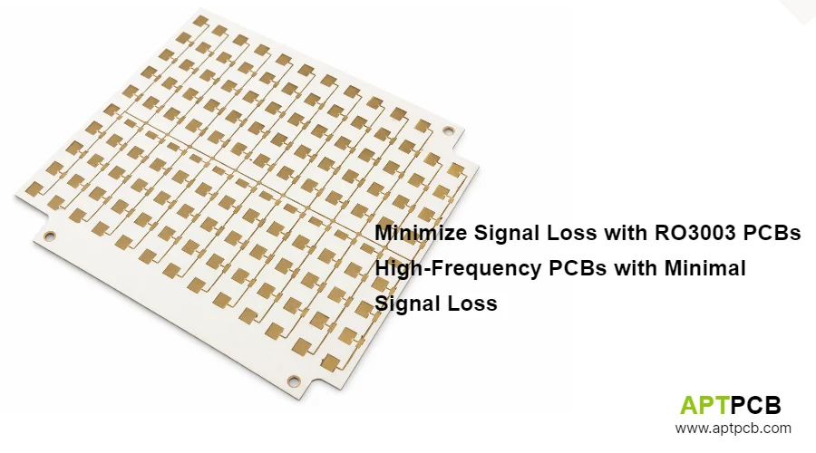
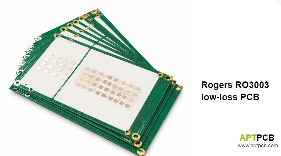
Rogers RO3003's Df of 0.0010 at 10GHz is among the lowest of any commercial substrate at production volumes. This guide starts from the link budget mathematics and works backward through the substrate, the trace design, and the fabrication process—grounding the meaning of Df 0.0010 in actual engineering outcomes.
The Link Budget Starts With the Substrate
A radar or communication system's performance margin is the difference between available signal power at the receiver and the minimum detectable signal. Everything in the system that consumes signal power—antennas, cables, PCB traces, connectors, switches—reduces this margin. The substrate contributes to this loss through two mechanisms: dielectric loss in the material surrounding the trace, and conductor loss from the surface roughness of the copper foil.
Both mechanisms depend on frequency. Both depend on trace length. Neither is fixed at design time—they are determined by the substrate material and the copper foil profile, which are specified before any trace is routed.
The Dielectric Loss Equation
The dielectric contribution to microstrip insertion loss follows:
α_d (dB/inch) ≈ 2.3 × f(GHz) × √Dk × Df
This formula has three variables: frequency (fixed by the application), Dk (fixed by substrate selection), and Df (fixed by substrate selection). For Rogers RO3003 (Dk = 3.00, Df = 0.0010):
| Frequency | Dielectric Loss on RO3003 |
|---|---|
| 10GHz (X-band) | ~0.040 dB/inch |
| 24GHz (automotive short-range radar) | ~0.095 dB/inch |
| 28GHz (5G NR mmWave) | ~0.112 dB/inch |
| 38GHz (Ka-band) | ~0.152 dB/inch |
| 60GHz (WiGig / industrial sensing) | ~0.239 dB/inch |
| 77GHz (automotive long-range radar) | ~0.307 dB/inch |
| 94GHz (W-band imaging) | ~0.375 dB/inch |
These are dielectric loss only—conductor loss adds to this, typically doubling total insertion loss for a well-designed microstrip trace on low-profile copper.
What Happens With a Higher Df Substrate
The comparison that makes Df 0.0010 concrete: for FR-4 (Df ≈ 0.020), the dielectric loss at 77GHz is approximately 7.2 dB/inch. For RO4350B (Df = 0.0037), it is approximately 1.22 dB/inch. For RO3003 (Df = 0.0010), it is 0.31 dB/inch.
On a 3-inch antenna feed network at 77GHz:
- FR-4: ~21.6 dB of dielectric loss → the entire link budget is consumed by the substrate before the signal reaches the antenna
- RO4350B: ~3.7 dB of dielectric loss → potentially workable for short feed networks but marginal for corporate-feed arrays
- RO3003: 0.93 dB of dielectric loss → leaves margin for connector loss, component variation, and manufacturing tolerances
The factor of 20 between FR-4's Df and RO3003's is not an incremental improvement—it is the difference between a non-functional design and a working one at 77GHz. Beyond the Df advantage, RO3003's Dk of 3.00 is also meaningfully lower than most competing substrates, which further reduces dielectric loss through the √Dk term in the formula. That compound effect—low Dk and low Df together—is what makes RO3003's insertion loss performance genuinely distinct at millimeter-wave frequencies.
What Low Dielectric Loss Enables in System Design
Low substrate loss is not an end in itself. It is a resource that can be spent in several ways, depending on what the system design is optimized for:
Longer Feed Networks at the Same Loss Budget
For a phased-array antenna with a corporate feed structure, the feed network must distribute signal from the RFIC transmitter to every antenna element. In a 16-element array, the outermost elements may be 30–40mm from the feed point. On FR-4 at 77GHz, this distance is unsupportable—signal reaches the outer elements with no useful power. On RO3003, 40mm of feed network costs approximately 0.5 dB of dielectric loss—within a reasonable link budget for an automotive radar.
Low-loss PCB material directly determines the maximum physical aperture size of a planar array at any given frequency—which determines angular resolution. Engineers designing arrays can trade the loss savings from RO3003's Df directly into array aperture.
Lower Required RFIC Transmit Power
For a fixed detection range requirement, reducing feed network loss by 1 dB allows the RFIC transmitter to operate 1 dB lower in output power. This is not a trivial trade: RF power amplifier linearity, efficiency, and thermal load are all functions of output power. A 3 dB reduction in transmit power requirement can reduce thermal load by 50%, enabling a smaller power amplifier with lower heat generation and lower cost. In a battery-powered application (drone radar, portable sensing), the power reduction extends operating time directly.
Better Receive Noise Figure
On the receive chain, every dB of insertion loss in the signal path before the first low-noise amplifier (LNA) adds 1 dB to the system noise figure. A feed network with 1 dB of insertion loss on the receive path raises the system noise figure by 1 dB—requiring either a lower-NF LNA (more expensive, harder to qualify) or accepting worse receiver sensitivity.
A low-loss substrate reduces this pre-LNA loss. At 77GHz, the difference between RO3003's 0.31 dB/inch and RO4350B's 1.22 dB/inch on a 2-inch receive feed is 0.62 dB vs. 2.44 dB. The 1.82 dB difference in pre-LNA insertion loss translates directly into 1.82 dB worse noise figure if the substrate is changed—which translates into reduced target detection range for small radar cross-section objects.
Relaxed RFIC Specifications
When the PCB substrate absorbs less signal power, the RF integrated circuits driving those lines can operate at lower output power and receive more signal power than they would on a higher-loss substrate. This can shift the design from a more expensive high-power RFIC to a standard-power device, or allow the receive chain to reach required sensitivity with one fewer LNA stage—a direct component count and cost reduction.
Conductor Loss: The Other Half of the Low-Loss Story
Specifying a low-Df substrate like RO3003 delivers the dielectric loss component of the link budget. Conductor loss is a separate mechanism, driven by the surface roughness of the copper foil and the skin effect at high frequencies. A designer who specifies RO3003 for its Df and then doesn't specify copper foil profile has addressed half the problem.
At 77GHz, the skin depth in copper is approximately 0.24 μm. Standard electrodeposited copper has RMS roughness Ra ≈ 5–7 μm. The ratio of roughness to skin depth is approximately 20–30:1, meaning current cannot follow the straight trace path—it must follow the surface contours. The effective resistance increases, and the conductor insertion loss increases by 30–40% compared to a smooth surface.
Low-profile ED copper (Ra ≈ 1.5 μm) reduces this ratio to approximately 6:1. Conductor loss premium over an ideal surface is approximately 10–15%. For a 77GHz program, total insertion loss on a low-profile copper microstrip trace (dielectric + conductor combined) is approximately:
- 0.31 dB/inch dielectric (RO3003 at 77GHz)
- ~0.35 dB/inch conductor (low-profile copper, 10 mil trace, estimate)
- Total: ~0.65 dB/inch
With standard copper (Ra ≈ 6 μm), conductor loss rises to approximately 0.47 dB/inch, giving a total of ~0.78 dB/inch—20% higher overall. On a 3-inch feed network, the difference is 1.95 dB vs. 2.34 dB. Not catastrophic, but for a receive feed network, 0.4 dB of unnecessary insertion loss directly degrades noise figure.
Low-profile copper must be specified in the laminate order. It is a Rogers Corporation procurement specification, not a fabrication step. APTPCB sources RO3003 for all mmWave programs with low-profile ED copper or RTF as standard—but this must be confirmed explicitly in the RFQ, because default laminate from Rogers ships with standard foil unless otherwise specified.
Dk 3.00: Why the Dielectric Constant Value Also Reduces Loss
The dielectric loss formula includes a √Dk term. This means that at fixed Df, a lower-Dk substrate produces less dielectric loss per unit length. RO3003's Dk of 3.00 is lower than many competing substrates:
| Substrate | Dk | Df | Relative Dielectric Loss at Same Frequency |
|---|---|---|---|
| Rogers RO3003 | 3.00 | 0.0010 | 1.00× (baseline) |
| Rogers RO4350B | 3.48 | 0.0037 | ~3.98× |
| Rogers RO4003C | 3.38 | 0.0027 | ~2.86× |
| Generic PTFE (Dk |
~3.0 | ~0.003 | ~3.00× |
| FR-4 (Dk |
~4.2 | ~0.020 | ~23.6× |
The Dk advantage compounds the Df advantage. RO3003 is not just a low-Df substrate—it is a low-Dk, low-Df substrate, and both properties contribute to its best-in-class insertion loss performance at GHz frequencies.
The lower Dk also produces wider trace widths for the same impedance target, which is a fabrication benefit: a 50Ω microstrip trace on 10 mil RO3003 is approximately 10 mil wide, while the same impedance on a 3.48 Dk substrate would be approximately 8 mil wide. Wider traces etch more consistently, are more tolerant of LDI registration variation, and are easier to inspect with 3D AOI.
Locating Loss: What TDR and VNA Measurements Reveal
When a completed RO3003 low-loss PCB shows more insertion loss than the simulation predicted, there are three places to look:
Dielectric loss. Measured by comparing the Df of the actual substrate to the simulation input. TDR cannot isolate dielectric loss from conductor loss. VNA S21 measurement through a long trace coupon, compared against a short trace coupon, yields the per-unit-length insertion loss—which can be compared against the simulation's predicted value.
Conductor loss from copper roughness. If the fabrication used standard copper instead of low-profile, conductor loss will be 30–40% higher than a simulation built with low-profile foil roughness parameters. This is a specification-at-order-time issue, not a fabrication error—but it shows up as systematic excess insertion loss across all traces on the board.
Impedance mismatch reflections. Trace width variation (from etch process variation or LDI registration errors), via transitions, and connector launches all introduce impedance discontinuities. Each discontinuity reflects a fraction of the signal power, which shows up as excess "loss" in S21 measurements. TDR testing on production panel coupons identifies whether trace widths are within the ±10% specification. APTPCB's LDI process achieves ±10% trace width standard with ±5% achievable for tight-tolerance structures.
For programs where insertion loss margin is tight—receive-path feed networks where every 0.1 dB matters—requesting TDR coupon data and first-article VNA data as part of the prototype deliverables establishes the actual insertion loss baseline before any component-level uncertainty is introduced. The fabrication process controls that minimize insertion loss variation—from drill parameters through plasma treatment to via plating copper thickness—are covered in the RO3003 PCB fabrication guide.
Design Choices That Determine Realized Insertion Loss
Specifying Rogers RO3003 establishes the substrate's contribution to insertion loss. The design choices below determine how much of that substrate advantage is actually realized in hardware:
Minimize feed network length. Every inch of trace adds loss. The most powerful low-loss strategy is not substrate selection—it is placing the RF source as close to the antenna aperture as possible. Substrate selection determines the loss per inch; trace length determines how many inches of loss are accumulated.
Use outer-layer microstrip where probing and inspection are needed. Buried stripline has slightly lower loss per unit length (shielded geometry reduces radiation loss), but the inaccessibility of the traces means insertion loss cannot be verified by probing and any fabrication-induced variation must be inferred from full-board measurements.
Specify ImAg surface finish. ENIG adds a 3–5 μm nickel underlayer with ~4× higher resistivity than copper. At 77GHz, this layer increases conductor insertion loss by approximately 0.1–0.2 dB/inch. For receive-chain feed networks where noise figure margin is limited, this penalty is significant. Immersion Silver (ImAg) deposits 0.1–0.2 μm of silver and is effectively transparent to RF current. ImAg does require tighter handling protocols—shorter shelf life after opening the moisture barrier bag and nitrogen reflow to prevent tarnishing—so the surface finish decision should be aligned between design and assembly teams before the board is ordered.
Avoid stub-creating via transitions. Via stubs create resonant nulls in the insertion loss spectrum. A transmission null at any frequency within the operating band effectively sets S21 at that frequency to −∞ dB—far more damaging than any Df-driven loss. Stub elimination by blind via, back-drilling, or stackup design should be addressed before layout, not treated as a post-measurement fix.
Low-Loss PCB as a System Specification
The practical value of Rogers RO3003's Df 0.0010 is not in the material spec itself—it is in what that property allows a system designer to guarantee to their customer. When a 77GHz radar is specified to detect a 1 m² target at 150m in −40°C conditions, the engineer signing the performance specification needs to know that the PCB substrate won't be the variable that causes the radar to fail at the corner of the operating envelope.
RO3003's combination of Df 0.0010, Dk 3.00 ± 0.04, and TcDk −3 ppm/°C converts the substrate from a variable into a constant in the link budget calculation. The radar's insertion loss at −40°C is calculably close to its insertion loss at +85°C. The board-to-board variation in feed network loss is bounded by ±0.04 Dk tolerance. The margin consumed by the substrate in production is predictable, not stochastic.
For a system that must be certified, qualified, and warranted in the field, that predictability is as valuable as the raw performance number. Before Gerbers are finalized, it's worth running the insertion loss model for your specific feed network length and frequency—APTPCB's engineering team can provide substrate-level loss estimates and copper foil profile recommendations for any preliminary stackup, without requiring a complete layout to do so.