Apply standard FR-4 fabrication parameters to a Rogers RO3003 board and you'll get melted resin smeared across via walls, copper plating that peels off at the first thermal stress, and panels warped beyond SMT assembly tolerance. Not because the process was careless—but because RO3003 is a fundamentally different material that breaks every assumption FR-4 fabrication is built on.
This article is a process-level walkthrough of what those differences are and how each one gets handled in a facility equipped for PTFE substrates.
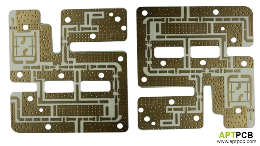
Why RO3003 Breaks Standard Fabrication
Three material properties drive every process deviation:
1. Low surface energy (~18 dynes/cm). PTFE is hydrophobic. Standard alkaline permanganate desmear chemistry—designed for epoxy resins—beads up and runs off the PTFE via wall without activating it. The copper seed layer can't bond, so you get plating voids.
2. Thermoplastic behavior under friction. Unlike thermoset FR-4, PTFE softens under heat. High-speed drilling generates enough friction to melt and smear the fluoropolymer across the internal copper interconnects before the drill has finished the hole.
3. Abrasive ceramic loading. The same ceramic particles that stabilize RO3003's dielectric constant will destroy a carbide drill bit in a fraction of the hits it would last on glass-epoxy.
These three behaviors are a direct consequence of what RO3003 is: a ceramic-loaded PTFE composite engineered for Dk stability, not for machinability. RO3003's Z-axis CTE of 24 ppm/°C—a property explained in detail in the RO3003 material properties overview—is also what drives the IPC Class 3 plating requirement; it's worth reading before evaluating via plating specifications from any fabricator.
Each of these requires a specific solution, applied in sequence.
Step 1: Drilling—Shear, Don't Melt
On FR-4 lines, spindle speeds of 120,000–150,000 RPM are standard. On PTFE, those speeds generate enough friction to melt the fluoropolymer before the drill can cut it cleanly. The molten PTFE smears across the copper foil on the inner layers—a defect that downstream chemistry cannot remove.
The fix is counterintuitive: slow the spindle down, and increase the chip load (infeed rate). You want the drill to shear the material aggressively rather than grind through it slowly.
APTPCB's PTFE drilling parameters:
- Spindle speed: 60,000–80,000 RPM (roughly half the FR-4 rate)
- Chip load: Increased infeed to ensure positive material removal rather than friction burnishing
- Hit count limit: Under 500 hits per drill bit (vs. 2,000+ for FR-4). The ceramic fillers in RO3003 dull carbide edges rapidly. A dull drill doesn't cut—it tears. Torn hole walls mean rough surfaces that interfere with plating adhesion even after plasma treatment.
The result of properly drilled RO3003 holes is clean, smooth wall surfaces with no white PTFE smear visible on the internal copper layers. Microsection inspection at this stage catches any smear before proceeding.
Step 2: Vacuum Plasma Desmear—The Mandatory Deviation
This is the step that eliminates most general-purpose PCB shops from the RO3003 market.
Standard desmear uses alkaline permanganate chemistry: it swells and attacks epoxy resin residue, leaving a micro-roughened surface the electroless copper seed layer can bond to. On PTFE, this chemistry has essentially no effect. PTFE's surface energy (~18 dynes/cm) is simply too low for the wet chemistry to wet, react, and prepare the surface.
Without adequate surface preparation, the palladium catalyst that initiates electroless copper plating won't activate properly on the PTFE via wall. The copper deposits incompletely—wedge voids, partial barrel coverage, plating that separates from the wall under the first thermal stress event.
Vacuum plasma surface modification replaces wet desmear entirely for PTFE:
Chamber loading: Drilled panels go into a vacuum plasma reactor. Chamber pressure is pumped down.
Gas chemistry: A metered mixture of Carbon Tetrafluoride (CF₄) and Oxygen (O₂) is introduced. The CF₄/O₂ ratio is tuned for RO3003's specific ceramic/PTFE composition.
Ion bombardment: An RF electromagnetic field energizes the gas to plasma state. Reactive CF₄ ions physically bombard the via wall, etching away the outermost layer of the PTFE matrix and creating micro-scale surface roughness that provides mechanical interlocking for the copper deposit.
Chemical activation: Simultaneously, oxygen plasma strips fluorine atoms from the polymer backbone. The exposed carbon reacts with oxygen to form hydrophilic polar functional groups (hydroxyl -OH, carbonyl -C=O) on the surface. Surface energy rises dramatically—from ~18 dynes/cm to values compatible with the subsequent palladium catalyst and electroless copper chemistry.
After plasma treatment, the via wall behaves as if it were an activated epoxy surface. The palladium catalyst wets uniformly. Electroless copper deposits across the entire wall with no voids.
This equipment cannot be outsourced. Moving drilled panels to an external facility for plasma treatment introduces handling risk, delays, and removes process traceability. APTPCB's in-house plasma chambers allow process parameters to be logged and linked to each panel's manufacturing record.
Step 3: Laser Direct Imaging for RF Trace Accuracy
At 77GHz, trace width directly determines impedance. A ±0.5 mil variation on a 10 mil trace produces roughly ±5% impedance error—the edge of acceptable tolerance for most 77GHz RF designs.
Standard phototool UV imaging has limited resolution and is sensitive to panel bow, lamp aging, and UV intensity variation across the panel. LDI (Laser Direct Imaging) exposes dry film photoresist directly from the digital Gerber file—no phototool intermediate, and registration is image-to-image rather than relying on tooling holes.
APTPCB's LDI process achieves ±10% trace width tolerance standard, with ±5% for tight-tolerance RF layers. Etch compensation factors—calculated from measured undercut data for the specific copper foil type and thickness on each RO3003 core—are applied before imaging to ensure the final etched trace width matches design intent.
Step 4: Hybrid Lamination—RO3003 + FR-4 CTE Management
Building a 6- or 8-layer board entirely from RO3003 is economically impractical for most commercial programs. The standard approach is a hybrid stackup: RO3003 on the outer RF layers where signal integrity matters, fused to high-Tg FR-4 for internal routing and power distribution. This typically reduces raw material cost by 30–45% while preserving 77GHz performance on the critical layers.
The fabrication challenge: RO3003 (PTFE thermoplastic) and FR-4 (thermoset epoxy) have different thermal expansion behaviors, different flow characteristics under heat and pressure, and don't bond to each other without appropriate intermediary films. The core thickness selection, copper foil profile, blind via aspect ratios, and POFV array geometry in a custom hybrid RO3003 stackup all determine both fabrication yield and final RF performance—stackup decisions that have cascading effects on every downstream process step.
Three process controls make hybrid lamination reliable:
Symmetric Copper Retention on FR-4 Inner Layers
During lamination and cooling, the FR-4 inner layers must act as mechanical stiffeners to counteract the thermal stress of the PTFE outer layers. If significant copper has been etched away from inner layers—as naturally happens in high-density routing—the panel loses mechanical balance.
APTPCB's DFM review mandates 75–80% minimum copper density on FR-4 ground and power planes in hybrid RO3003 stackups. Where routing density would reduce this, copper pour or hatched fill is added in non-signal areas to restore planarity.
Low-Flow, High-Tg Bonding Films
Standard FR-4 prepreg flows too aggressively under lamination pressure and can deform fine RF traces on adjacent RO3003 layers. Pure PTFE bonding films (such as Rogers 3001) require temperatures above 220°C—which damages most FR-4 inner layer materials.
The solution is specialized low-flow, high-Tg (>170°C) thermoset prepregs that cure within the standard lamination temperature window without flowing into the RF trace areas, and whose glass transition temperature remains above the peak reflow temperature the assembly will experience.
Controlled Isothermal Cooling: ≤2°C per Minute
This is the most common failure point in hybrid lamination. During the press cycle (above 180°C), the FR-4 and RO3003 layers expand at different rates. If the press cools quickly, they contract at different rates, locking in internal shear stress. The result is a warped, twisted panel—sometimes called the "potato chip effect"—that's incompatible with SMT pick-and-place equipment.
APTPCB's lamination presses use extended isothermal holds followed by a strictly controlled cooling ramp of ≤2°C per minute. This allows polymer chains in both materials to relax uniformly before the panel reaches room temperature, equalizing internal stress.
Target: IPC-A-600 bow and twist ≤0.75%. APTPCB's controlled cooling process consistently achieves <0.5% on hybrid panels.
Step 5: IPC Class 3 Via Plating
The plated through-hole is the most mechanically stressed feature on an automotive radar board. During lead-free SMT reflow (245–260°C peak), the Z-axis thermal expansion of the RO3003 dielectric pushes outward on the copper inside every via barrel. Thin copper cracks under this stress—creating an open circuit that may survive incoming inspection but fail after a few thermal cycles in the vehicle.
APTPCB's plating standards for RO3003 automotive boards:
| Parameter | IPC Class 2 Baseline | APTPCB RO3003 Standard |
|---|---|---|
| Average hole wall copper | 20 μm | 25 μm minimum |
| Any single measurement | 18 μm minimum | 20 μm minimum |
| Resin recession | ≤25 μm | ≤10 μm |
| Wedge voids | ≤1 per hole | Zero tolerance |
For via-in-pad (POFV) structures beneath RF transceiver ICs—a configuration common in high-density 77GHz modules—the requirements extend to wrap plating of ≥12 μm onto the surface pad to prevent pad cratering during thermal shock. HDI design considerations for via-in-pad structures on standard high-density boards carry over directly to RO3003 hybrid stackups where RF ICs land on POFV pads.
The 25 μm average provides mechanical reserve against Z-axis CTE-induced fatigue. The zero-void standard requires the plasma activation to have worked correctly—incomplete activation produces partial plating, and partial plating produces voids.
Every batch releases with a microsection cross-section report: measured copper thickness at multiple points in the via barrel, photographed evidence of no wedge voids, and visual confirmation of the plasma-treated PTFE interface with seamless copper adhesion.
Step 6: Surface Finish Options
| Finish | Performance at 77GHz | Shelf Life | Key Consideration |
|---|---|---|---|
| Immersion Silver (ImAg) | Excellent — flat deposit preserves copper roughness | 12 months sealed MBB | Requires sulfur-free packaging |
| ENIG | Good — nickel layer adds minor insertion loss | 12 months | Acceptable for 24GHz and below |
| HASL | Not suitable | — | Uneven surface disrupts fine-trace impedance |
For 77GHz RF layers, ImAg is the standard recommendation. The thin deposit (0.1–0.2 μm) is effectively transparent to RF current, which rides on the underlying copper surface.
Process Validation Before Release
Before any RO3003 batch ships or goes to assembly:
- TDR impedance test: High-bandwidth time-domain reflectometry on production test coupons validates 50Ω and 100Ω differential lines to ±5% tolerance
- 288°C solder float, 3× cycles: Thermal stress to IPC Class 3 specification; microsection confirms no delamination at the RO3003/FR-4 interface and no barrel fracture
- Microsection report: Cross-section photographs with measured copper thickness at top, middle, and bottom of sample via barrels; void classification
- Full electrical test: 100% continuity and isolation on every panel
This documentation package—TDR data, microsection report, Rogers COC—is what should accompany every production batch from a qualified fabricator. If a manufacturer cannot produce TDR data and microsection reports on request, their process control is not adequate for automotive programs.
For a structured audit framework covering IATF 16949 verification, in-house plasma equipment, ESS reliability testing, and material traceability when evaluating any new fabricator, the RO3003 PCB manufacturer qualification guide provides the specific verification questions and documentation requests that separate a genuine PTFE process from a claimed one.
Submit your RO3003 Gerber files to APTPCB for a no-cost DFM review covering drilling parameters, stackup thermal management, and IPC Class 3 plating requirements before committing to prototype fabrication.
Normative References
- Plasma desmear chemistry and PTFE surface energy (18 dynes/cm) from IPC-2226 Sectional Design Standard for HDI Printed Boards.
- Plating thickness, void acceptance, and bow/twist criteria per IPC-6012 Class 3 and IPC-A-600K Acceptability of Printed Boards.
- Drill parameters and lamination cooling rates from APTPCB's Automotive Radar PTFE Fabrication Control Plan (2026).