The microwave filter designer's argument for RO3006 is architectural, not electrical. At 10 GHz on RO3003, a coupled-line filter resonator element is roughly 5.3 mm long—which is acceptable until the assembly includes multiple filter sections, a diplexer, and a power divider that must all fit within a 40×40mm module envelope. On RO3006, that same resonator is approximately 4.0 mm. Across a complex microwave circuit, those millimeters compound into the difference between a design that fits and one that doesn't.
This is where Dk 6.15 earns its place. RO3006's dissipation factor of 0.0020—twice that of RO3003—is a real insertion loss penalty that must be budgeted honestly. But for the class of microwave circuits where physical envelope is the binding constraint rather than minimum loss, RO3006 allows designs that cannot be realized on a lower-Dk substrate within the available space.
The Case for Higher Dk in Microwave Circuit Design
Distributed-element microwave circuits—coupled-line filters, branch-line couplers, stub-tuned matching networks—are built from transmission line sections whose physical length is a specified fraction of the guided wavelength. The guided wavelength at any frequency depends directly on the substrate Dk:
L_physical = λ_guided × (electrical length / 360°)
At 10 GHz, a quarter-wave section on RO3003 (Dk = 3.00) is approximately 5.3 mm. On RO3006 (Dk = 6.15), the same quarter-wave is approximately 4.0 mm—25% shorter. For a 3-resonator Chebyshev bandpass filter, this reduces the resonator chain from approximately 16 mm to approximately 12 mm, with proportional reductions in coupled-line gap spacings and line widths.
The Rogers RO3006 microwave PCB design context covers the broader microwave substrate landscape. Within that landscape, RO3006's role is specific: it serves designs where the spatial constraint matters more than the insertion loss penalty, and where the operating frequency is typically in the range where RO3006's Df of 0.0020 remains within link budget.
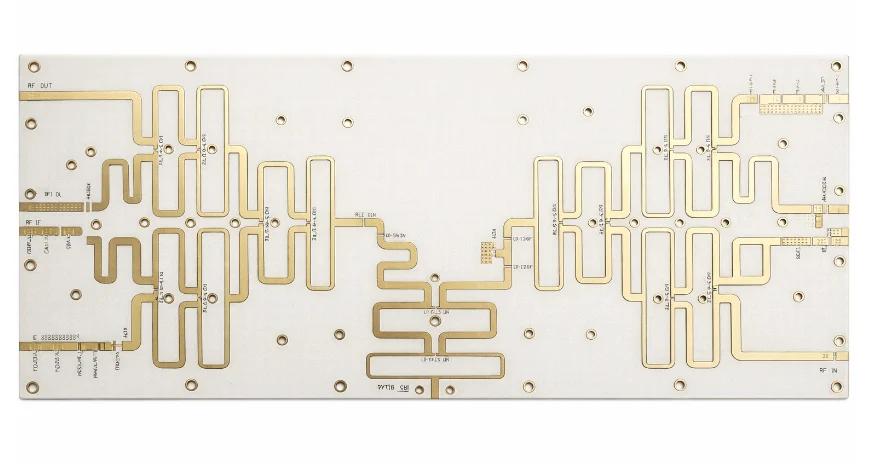
Bandpass Filter Design on RO3006
Resonator Sizing and Compactness
For a coupled-line bandpass filter, the resonator element length is a quarter-wave at the center frequency. At key microwave frequency bands:
| Frequency | Quarter-wave on RO3003 | Quarter-wave on RO3006 | Reduction |
|---|---|---|---|
| 5 GHz (C-band) | ~10.6 mm | ~8.0 mm | ~25% |
| 10 GHz (X-band) | ~5.3 mm | ~4.0 mm | ~25% |
| 18 GHz (Ku-band) | ~2.9 mm | ~2.2 mm | ~25% |
For a module with a fixed height or length constraint—a satellite receiver LNB assembly, a radar signal processing rack unit, an electronic warfare subsystem—these 25% linear reductions in resonator elements can make the difference between fitting the required functionality and needing a larger enclosure.
Coupled-Line Geometry on Dk 6.15
The coupled-line filter geometry on RO3006 uses narrower lines and tighter gaps than on RO3003 for the same coupling specification. For a 50Ω coupled-line structure at 10 GHz on a 10 mil core:
- On RO3003: trace width approximately 10 mil, gap approximately 10–20 mil depending on coupling coefficient
- On RO3006: trace width approximately 6 mil, gap approximately 6–12 mil
These narrower geometries impose tighter fabrication requirements. A 6 mil gap with ±1 mil etch variation produces ±17% coupling coefficient variation—directly affecting filter passband flatness and stopband rejection consistency. LDI imaging with etch compensation calibrated specifically to RO3006's copper foil and core thickness is mandatory for microwave filter programs; standard UV phototool exposure cannot hold these tolerances.
Insertion Loss and Q-Factor Trade
The unloaded Q-factor of a distributed resonator relates inversely to the substrate loss tangent. RO3006's Df of 0.0020 produces roughly half the unloaded Q of RO3003 (Df 0.0010) at the same frequency and geometry. For filter designs:
- Narrowband filters (fractional bandwidth <1%): Lower Q on RO3006 increases passband insertion loss meaningfully. For narrowband filter applications requiring minimum insertion loss, RO3003 is the correct substrate.
- Wideband filters (fractional bandwidth >5%): The Q requirement is relaxed; RO3006 can meet the insertion loss specification while delivering smaller physical dimensions.
- Filter banks and multiplexers: Where multiple filters share a housing with a fixed footprint, the compactness of RO3006 may enable accommodation of more channels within the space—trading some per-channel loss for higher channel density.
Diplexer Applications on RO3006
A diplexer routes two frequency bands through a common port: one to the transmit chain, one to the receive chain, or two different operating bands to separate processing paths. The diplexer body consists of two filter sections connected at a common junction point.
On RO3006, both filter sections are proportionally smaller. A diplexer designed for X-band transmit (8.5 GHz) and Ku-band receive (12.5 GHz) that would occupy approximately 30×20mm on RO3003 fits within approximately 22×15mm on RO3006—about 45% smaller in total area. For housing-constrained applications—satellite terminal front ends, airborne radar subsystems, vehicle-mounted electronic warfare modules—this area reduction directly determines packaging density.
Junction design on RO3006. The T-junction connecting the common port to the two filter branches introduces a shunt capacitance that must be compensated. On RO3006, the shorter guided wavelength means this junction occupies a larger fraction of the electrical length at the design frequency, and compensation geometry (notch cuts, pad shape modifications) must be redesigned relative to RO3003—borrowed compensation geometries from RO3003 designs will not perform correctly on RO3006. Full-wave EM simulation of the junction region is necessary for accurate first-prototype performance on RO3006 diplexers.
Phase Shifter Design on Dk 6.15
Switched-line phase shifters select between two transmission line paths of different electrical length. The physical length difference ΔL for a phase shift Δφ is:
ΔL = Δφ × λ_guided / 360°
At 10 GHz, for a 45° phase shift on RO3006: ΔL ≈ (45/360) × 15.9 mm ≈ 2.0 mm
The same phase shift on RO3003 requires: ΔL ≈ (45/360) × 21.3 mm ≈ 2.7 mm
A 4-bit phase shifter (22.5°, 45°, 90°, 180°) requires four such path length pairs. On RO3006, the total footprint of the switching path length differences is approximately 25% smaller than on RO3003. In a densely integrated beamforming network for a phased-array module, this reduction compounds across the full set of phase shifter bits for every element in the array.
For analog phase shifters using varactor-loaded transmission lines or ferroelectric thin films, the substrate Dk also affects the loaded-line phase velocity and the varactor capacitance required for a given phase shift. Higher substrate Dk shifts the varactor loading ratio required for a specified phase-velocity ratio, which must be accounted for in the phase shifter synthesis.
Thermal Management in High-Power Microwave Modules
Power amplifier stages in microwave transmit modules—including solid-state power amplifiers (SSPAs) and GaN power MMICs—dissipate heat that must be extracted through the PCB. RO3006's ceramic loading is higher than RO3003's, and the PTFE-ceramic composite's thermal conductivity increases with higher ceramic fraction. Consult the current Rogers Corporation datasheet for the precise thermal conductivity value to use in thermal simulation.
In practice, neither RO3006 nor RO3003 provides useful lateral heat spreading. Heat must be extracted vertically through POFV copper via arrays beneath the device thermal pad—routed to a chassis heat sink or cold plate. The POFV design approach is identical to that used for RO3003 power stages: ≥50% thermal pad coverage with 0.3mm filled vias at 0.6mm pitch, POFV cap plating planarity within ±10 μm. The exact geometry, fill specification, and 3D X-ray void acceptance criteria are covered in the RO3003 PCB manufacturing and thermal management guide; all of those parameters apply equally to RO3006 power stages.
For turnkey microwave module production that integrates bare board fabrication with SMT assembly under a single quality management system, APTPCB's PCB assembly and manufacturing service covers the full chain from Rogers RO3006 material receipt through 3D X-ray inspection of assembled power stages.
Fabrication Controls Specific to Microwave-Grade RO3006 Programs
For filter and diplexer programs where center frequency, passband ripple, and rejection are production specifications—not just first-article targets—additional process controls must be specified at the RFQ stage:
Dk lot tracking. Rogers RO3006's Dk tolerance of ±0.15 means filter center frequency can vary by up to ±1.2% across production lots. For a 10 GHz filter, this is ±120 MHz. Lot-level Dk tracking, enabled by the MES lot traceability system, allows the fabricator to report which Rogers lot was used for each production batch. Correlation between lot Dk value and measured filter center frequency enables incoming inspection-based yield screening for tightest-specification programs.
TDR coupon confirmation of coupled-line geometry. Standard TDR coupon structures measure 50Ω single-ended or 100Ω differential impedance. For coupled-line filter programs, additional coupon structures that allow verification of the even-mode and odd-mode impedances of the coupled section provide the fabrication-level quality gate that a 50Ω TDR alone cannot give.
First-article VNA characterization. For every new coupled-line or diplexer design on RO3006, a full two-port S-parameter measurement across the filter passband and stopbands—compared directly against the EM simulation—confirms that fabricated hardware matches the design intent. Deviations that exceed the link budget requirement trigger investigation before production release, not after field deployment.
Working With APTPCB on RO3006 Microwave Programs
APTPCB processes RO3006 on dedicated PTFE fabrication lines with in-house vacuum plasma capability, LDI imaging, and controlled hybrid lamination. For microwave filter and array programs, we provide:
- DFM review within 24 hours of Gerber submission, covering coupled-line geometry, via transitions, and hybrid stackup bow/twist management
- TDR impedance testing on every production panel
- First-article RF characterization support for filter qualification builds
- Rogers material COC with lot number and MES panel traceability as standard batch documentation
Contact APTPCB to discuss RO3006 core thickness availability, submit a filter design for DFM review, or request process qualification documentation for your microwave program.
Normative References
- Dk, Df specifications from Rogers Corporation RO3000® Series Circuit Materials Datasheet (current revision).
- Coupled-line filter synthesis per Matthaei, Young, Jones, Microwave Filters, Impedance-Matching Networks, and Coupling Structures, Artech House.
- POFV design per IPC-4761 Design Guide for Protection of Printed Board Via Structures.
- Plating and process requirements per IPC-6012 Class 3.