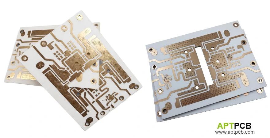
Here is the paradox at the center of every 77GHz radar manufacturing program: the substrate selected specifically for its RF performance is a thermal insulator. Rogers RO3003's dielectric properties are excellent. Its thermal conductivity is 0.50 W/m/K—which puts it roughly in the range of structural foam relative to what's needed beneath a radar transceiver IC running at full power.
This isn't a reason to avoid RO3003. It's a reason to understand exactly what the manufacturing process needs to do about it. That process starts upstream: the PTFE fabrication steps that produce the bare board—modified drilling parameters, vacuum plasma desmear, and controlled hybrid lamination cooling—determine whether the POFV thermal via arrays and copper structures that manage heat are built to spec before any component is assembled.
Understanding the Thermal Paradox
A 77GHz RFIC amplifier driving a phased-array radar can dissipate several watts into a package thermal pad smaller than a postage stamp. On a standard FR-4 board, that energy would spread laterally through the substrate—inefficiently, but somewhat. On RO3003 at 0.50 W/m/K, lateral spreading is essentially zero. Heat pools beneath the component.
The downstream consequences:
Gain compression: As junction temperature approaches the RFIC's maximum rating (typically 125–150°C for automotive-grade parts), amplifier gain compresses. Output power falls. In a 77GHz collision avoidance system, this means reduced detection range.
Phase drift: Although RO3003's TcDk is excellent at −3 ppm/°C, extreme localized temperatures above ~120°C induce Z-axis volumetric expansion in the surrounding dielectric, shifting the distributed capacitance of nearby antenna feed lines and introducing phase noise that degrades beam-steering accuracy.
Solder joint fatigue: Temperature gradients between a 120°C junction and a 40°C ambient 5mm away create cyclic mechanical shear on solder joints. Over thousands of thermal cycles, fatigue cracks develop.
The engineering solution is to design a conductive thermal path through the substrate before the component is assembled. That path is built from electroplated copper—398 W/m/K—and it runs vertically through the board.
POFV Thermal Via Arrays: Engineering the Z-Axis Heat Path
The standard approach for RO3003 radar boards is a Plated Over Filled Via (POFV) array positioned directly beneath the exposed thermal pad of the RF IC.
The mechanism: A dense array of copper-plated through-holes creates a vertical copper column from the component pad through the RO3003 core and into a metal chassis, cold plate, or internal thermal dissipation layer. Each copper via barrel conducts heat approximately 800× more efficiently than the surrounding dielectric. A well-designed array reduces thermal resistance under a high-power RFIC from the multi-hundred °C/W range (through dielectric alone) to 15–25°C/W depending on array density and chassis attachment.
Fill and planarization requirement: A hollow via can't be reliably soldered over. Solder paste that collapses into an unfilled via creates a void beneath the thermal pad—blocking the heat path and creating a localized hotspot. The fix is to fill via holes with thermally conductive epoxy resin, then plate copper over the filled surface (POFV), creating a flat solderable pad. APTPCB targets POFV surface planarity within ±10 μm of the surrounding copper. Deviations beyond this cause uneven paste volume distribution leading to voiding even with a well-designed stencil.
Typical sizing for 77GHz applications: For a QFN transceiver with a 3×3mm thermal pad, a 3×3 or 4×4 array of 0.3mm drilled vias at 0.6mm center-to-center pitch provides adequate thermal resistance. Via array coverage should be at least 50% of the thermal pad area. Validate with thermal simulation before layout finalization. Via geometry, fill specification, and cap plating planarity are among the fabrication-facing decisions covered in depth in the custom RO3003 PCB design and DFM process.
Surface Finish: Immersion Silver vs. ENIG at Millimeter-Wave Frequencies
At 77GHz, the skin effect concentrates current in the outermost 1–2 μm of the conductor. The surface finish is part of the RF signal path.
Immersion Silver (ImAg): At 0.1–0.2 μm deposit thickness, ImAg is electromagnetically transparent—RF current rides on the underlying copper surface. Solderability is excellent, and the flat, smooth morphology preserves trace impedance along RF feed lines.
ENIG: Deposits 3–5 μm of nickel beneath thin gold. Nickel's bulk resistivity is roughly 4× higher than copper. At 77GHz, this layer contributes approximately 0.1–0.2 dB/inch of additional insertion loss compared to ImAg. For a 3-inch antenna feed network, the penalty is measurable and real.
ImAg handling implications: Silver tarnishes when exposed to sulfur compounds or fingerprint oils. APTPCB ships all ImAg-finished RO3003 boards in sulfur-free protective paper, vacuum-sealed in Moisture Barrier Bags with desiccant and Humidity Indicator Cards (HIC). Sealed shelf life: 12 months. After opening: assemble within 5 working days.
SMT Assembly: Four Controls That Determine Reliability
The four controls below address the failure modes specific to RO3003 hybrid boards at the SMT stage. For programs requiring a complete process reference—including first article inspection, component co-planarity requirements, and the full 3D AXI voiding acceptance criteria—the RO3003 PCB assembly process guide covers each step from pre-bake through post-reflow validation.
1. Moisture Pre-Baking Before Line Entry
RO3003 absorbs almost no moisture (0.04%). But the hybrid RO3003/FR-4 boards standard in commercial 77GHz programs use FR-4 inner layers that are hygroscopic. Absorbed moisture that reaches the dielectric-copper interface during a 250°C reflow cycle can flash to steam, causing internal delamination and via barrel cracking.
APTPCB pre-bakes all hybrid boards immediately before SMT assembly services begin: a controlled bake cycle that drives absorbed moisture from FR-4 layers without aggressively oxidizing the ImAg finish. Boards enter the SMT line within minutes of bake completion.
2. Window-Pane Stencil Design for Thermal Pads
This is the detail that most often determines whether thermal pad voiding passes or fails 3D X-Ray inspection.
A standard full-aperture stencil prints a single large solder deposit over the thermal pad. When solder melts during reflow, outgassing flux is trapped under the molten pool. It nucleates as voids that block the POFV thermal via array below.
The window-pane stencil divides the thermal pad aperture into a grid of smaller segments separated by paste-free web strips (typically 0.15–0.20mm wide). During reflow, flux vapor escapes through the web strips before solder solidifies. APTPCB consistently achieves under 10% thermal pad voiding using this approach—well below the IPC-A-610H Class 3 limit (30%) and our internal acceptance threshold (20%).
3. Nitrogen Reflow Atmosphere
Immersion Silver oxidizes at elevated temperatures. Solder powder develops surface oxides that increase viscosity, reduce wetting, and promote voiding.
APTPCB's reflow ovens for 77GHz radar modules operate with a pure nitrogen atmosphere, maintaining residual oxygen below 500 ppm. Nitrogen prevents ImAg tarnishing, lowers solder surface tension for better wetting over POFV surfaces, and allows peak temperature to be reduced to 245–250°C instead of 255–260°C—reducing cumulative thermal stress on the PTFE dielectric.
4. Controlled Reflow Profile
| Stage | Parameter |
|---|---|
| Preheat ramp | 1.5–2°C/second |
| Soak zone | 150–180°C, 60–90 seconds |
| Peak temperature | 245–250°C maximum |
| Time above liquidus | 30–45 seconds |
| Cooling rate | ≤3°C/second |
The controlled cooling rate prevents thermal shock to the PTFE/FR-4 hybrid interface—the same physical concern that drives slow cooling during bare board lamination.
3D X-Ray Inspection: Validating What Optical Inspection Can't See
Bottom-terminated RF components—QFN transceivers, BGAs, exposed thermal pads—have all their critical solder joints hidden beneath the package body. Standard AOI cameras see nothing below the package outline.
The limitation of 2D X-Ray: A 2D image collapses all layers into a single projection. The copper columns of the POFV via array and the solder layer above them appear superimposed. Accurate void measurement in the solder layer is not possible.
3D AXI with computed tomography: APTPCB's 3D Automated X-Ray Inspection systems capture the assembly from dozens of angles, reconstructing a high-resolution 3D model. Quality engineers slice horizontally through the exact solder layer—isolated from via copper above and board layers below—and measure void area, distribution, and position with precision.
APTPCB's RF Assembly Voiding Acceptance Criteria:
| Defect Type | IPC-A-610H Class 3 | APTPCB Internal |
|---|---|---|
| Total aggregate voiding on thermal pad | ≤30% | ≤20% |
| Any single isolated void | Not specified | ≤5% of pad area |
| Any void over a POFV thermal via | Not specified | Zero tolerance |
The zero-tolerance criterion for voids over thermal vias is APTPCB-specific. A void directly over a filled copper via severs the primary heat extraction path, creating a localized hotspot that thermal simulation cannot predict and no design margin can accommodate.
Pre-Assembly Moisture Control and IPC-1601 Compliance
The supply chain handoff between bare board fabrication and SMT assembly is where many reliability failures originate—failures that appear during thermal testing but trace back to inadequate moisture handling during transit or storage.
APTPCB's handling protocol:
- Pre-bake all hybrid boards to extract absorbed moisture from FR-4 layers
- Separate boards with sulfur-free interleaving paper
- Vacuum-seal in Moisture Barrier Bags with calibrated desiccant packs and active HIC cards
- Store at 18–22°C, <40% RH until line-side deployment
For high-volume production programs, co-locating bare board fabrication and SMT assembly under one roof eliminates the transit and storage exposure entirely. Boards move from the fabrication line to the SMT floor without leaving the climate-controlled building—the cleanest possible implementation of IPC-1601 moisture control.
The Turnkey Argument
The combination of POFV thermal design, window-pane stencil engineering, nitrogen reflow, and 3D AXI validation is a coherent system. When these processes are split across two suppliers—bare board fabrication at one facility, SMT assembly at another—accountability for failures fragments. If a board fails thermal testing due to excessive voiding, the assembly vendor attributes it to POFV surface planarity or ImAg degradation during shipping. The fabricator attributes it to the reflow profile. The OEM holds the liability.
Running the complete chain under one quality management system, with shared DFM records and IATF 16949 traceability, is the most reliable way to ensure the thermal design validated in simulation survives contact with the production line. Programs that scale from prototype to volume production also benefit from having fabrication process data—POFV planarity tolerances, ImAg finish thickness measurements, and reflow profile records—all accessible within a single mass production quality system rather than reconciled between two vendors. The full breakdown of RO3003 PCB cost drivers—including how turnkey integration affects unit pricing versus split-vendor models—provides the commercial context for this decision.
Contact APTPCB's manufacturing team to request a turnkey manufacturing quote for your RO3003 radar module or to schedule a thermal DFM review before your layout is finalized.
References
- RO3003 thermal conductivity from Rogers Corporation RO3000® Series Circuit Materials Datasheet (Rev 11.2023).
- SMT void acceptance per IPC-A-610H Acceptability of Electronic Assemblies, Class 3.
- Moisture handling per IPC-1601 Printed Board Handling and Storage Guidelines.
- Via-in-pad and POFV requirements per IPC-4761 Design Guide for Protection of Printed Board Via Structures.