A fabricator who can build Rogers RO3003 reliably is not automatically qualified for RO3006. Both materials share the same PTFE matrix and the same mandatory process architecture—vacuum plasma desmear, modified drilling, controlled lamination—but RO3006's higher ceramic loading raises the bar on two specific process parameters: drill bit wear rate is faster, and the trace widths required for RF structures are narrower. Either of these, if underestimated, produces the same class of failure: boards that pass electrical test and fail under thermal stress or produce RF performance outside specification.
This guide walks through the fabrication sequence for RO3006 step by step, identifying where the process deviates from FR-4, where it deviates from RO3003, and what documentation a qualified fabricator should be able to provide at each stage.
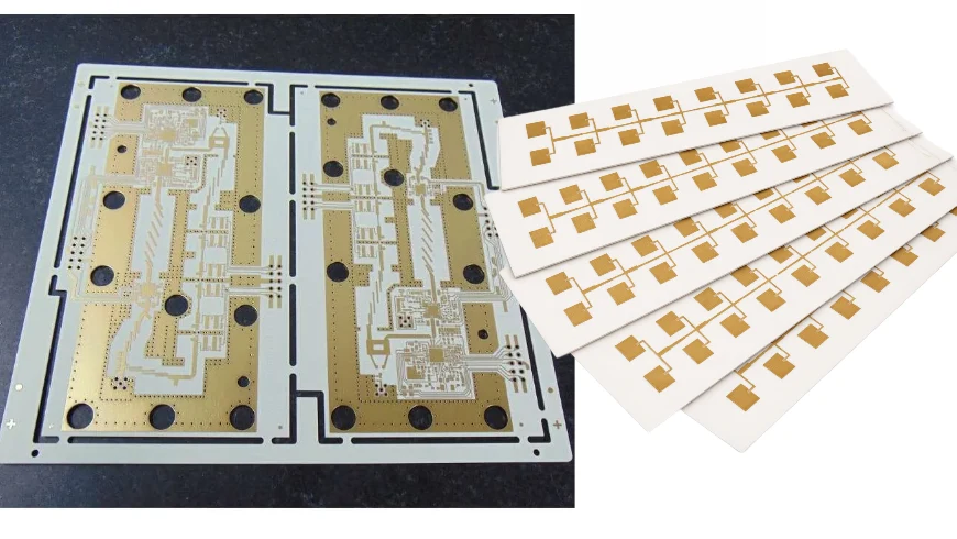
Why RO3006 Cannot Be Processed on a Standard FR-4 Line
Three material properties of RO3006 collectively break every assumption that FR-4 fabrication is built on:
PTFE surface energy (~18 dynes/cm). Like all RO3000 series materials, RO3006 uses a PTFE polymer matrix. PTFE's chemically inert surface cannot be activated by standard alkaline permanganate wet desmear—the chemistry used for epoxy-glass substrates. Without surface activation, palladium catalyst doesn't wet the via wall uniformly, electroless copper deposits incompletely, and via barrels contain plating voids that become open circuits under thermal cycling. Vacuum plasma desmear with CF₄/O₂ chemistry is the only effective solution.
Thermoplastic drilling behavior. PTFE softens under frictional heat. Standard FR-4 drilling spindle speeds of 120,000–150,000 RPM generate enough heat to melt and smear PTFE across the copper innerlayers before the drill exits the hole. Drill smear at inner copper layers cannot be removed by downstream chemistry and produces electrical opens at interconnect points.
Accelerated drill bit abrasion from ceramic loading. RO3006 contains more ceramic filler than RO3003—higher loading is required to achieve Dk 6.15 compared to RO3003's 3.00. That additional ceramic abrades carbide drill bits faster. The 500-hit limit already applicable to RO3003 must be applied at least as conservatively to RO3006, and process qualification on the actual material should establish the specific hit count limit for the facility's drill geometry and feed parameters.
The Rogers RO3003 PCB material overview covers the PTFE physics underlying these behaviors. RO3006 fabrication builds on that same framework; what's different are the magnitude of drill wear and the narrower trace geometry that follows from Dk 6.15.
Step 1: Incoming Material Verification
RO3006 laminate from Rogers Corporation carries a Certificate of Conformance (COC) with lot number, date code, and IPC-4103 compliance statement. Before any panel enters fabrication, incoming inspection must verify:
- COC lot number references a Rogers-authorized sourcing channel (direct from Rogers or named authorized distributor)
- Received core thickness matches the purchase order specification
- Copper foil profile matches the specification (standard ED vs. low-profile)—this is a laminate-level property that cannot be changed after the fact
For a fabrication process that must trace individual boards to the Rogers material lot in case of field failure, the COC lot number must be entered into the manufacturing execution system (MES) at incoming inspection and linked to every panel cut from that lot.
Step 2: Drilling—Shear, Not Melt
The modified PTFE drilling parameters that apply to all RO3000 series materials apply fully to RO3006:
- Spindle speed: 60,000–80,000 RPM (approximately half the standard FR-4 rate of 120,000–150,000 RPM)
- Infeed rate: Increased to ensure the drill shears the PTFE matrix cleanly rather than generating friction heat
- Hit count per bit: Limited to ≤500 hits due to ceramic filler abrasion—potentially fewer for RO3006 given its higher ceramic loading
The result of properly executed drilling is a clean, smooth via wall with no PTFE smear on the inner copper layers and no torn wall surfaces. A process engineer should inspect cross-sections from drilling qualification runs before committing production panels to the drill protocol.
One practical consequence of the low hit count limit: RO3006 programs have significantly higher drill bit consumption than FR-4 programs of equivalent via density. For a board with 500 vias per panel, a 500-hit limit means every drill bit is replaced after one panel. This is a real cost driver and should be factored into quotation from the start.
Step 3: Vacuum Plasma Desmear—Mandatory, Not Optional
After drilling, every RO3006 panel must go through vacuum plasma surface modification before electroless copper deposition. This step is the single most important process gate for PTFE substrates.
Why wet chemistry fails on RO3006. Alkaline permanganate desmear works by chemically swelling and etching epoxy resin residue from via walls. PTFE at ~18 dynes/cm surface energy is essentially inert to these reagents—the chemistry beads up and runs off the surface without activating it. A via wall that has not been plasma-treated will show partial copper deposition under the plating step: wedge voids, bare patches, or fully unplated zones that pass visual inspection under the drill hole but fail electrically after thermal stress.
The plasma process sequence for RO3006:
- Drilled panels are loaded into a vacuum plasma reactor and the chamber is evacuated
- A metered CF₄/O₂ gas mixture is introduced—the specific ratio must be optimized for the ceramic-PTFE composite composition of RO3006
- An RF electromagnetic field excites the gas to plasma state; CF₄ ions physically etch the outermost PTFE layer and create micro-scale surface roughness for mechanical interlocking
- Simultaneously, oxygen plasma creates hydrophilic polar functional groups on the exposed carbon backbone, raising surface energy from ~18 dynes/cm to values compatible with palladium catalyst adhesion
- After treatment, panels proceed immediately to electroless copper without atmospheric exposure that would reverse the surface activation
The plasma chamber must be in-house at the fabricator. Sending drilled panels to an external facility for plasma treatment breaks process traceability and introduces handling risk. Any prospective RO3006 fabricator who cannot show an in-house plasma chamber with a documented gas recipe for ceramic-PTFE materials does not have a qualified process for this substrate.
Step 4: LDI Imaging—Critical for Narrow RF Traces on Dk 6.15
At Dk 6.15, the 50Ω microstrip trace on a 10 mil core is approximately 5–7 mil wide—significantly narrower than the 9–11 mil trace width on the same core thickness with RO3003's Dk 3.00. This narrower geometry imposes tighter absolute tolerance requirements on the imaging and etching process.
Standard UV phototool imaging cannot reliably hold the trace width tolerances required for RF structures on RO3006. Phototool exposure is sensitive to lamp aging, UV intensity variation across the panel, and panel bow—each of which adds to trace width variability. For a 6 mil target trace, a ±1 mil variation is already a ±17% impedance error—outside the ±10% tolerance typical for controlled-impedance RF structures.
Laser Direct Imaging (LDI) exposes dry film photoresist directly from the Gerber file, without a phototool intermediate. LDI achieves ±10% trace width tolerance on standard RF structures and ±5% on tight-tolerance structures when etch compensation factors are calibrated from measured copper undercut data.
For RO3006 programs, LDI is not an upgrade—it is a process requirement for RF outer layers. The etch compensation factor for RO3006 must be characterized on the specific copper foil profile and weight being used. A fabricator who uses RO3003-calibrated etch compensation factors on RO3006 without recalibrating will produce trace widths that deviate from the design intent. This is the single most common source of first-prototype impedance failures on RO3006 programs that come from shops experienced with RO3003 but new to the higher-Dk material.
Step 5: Hybrid Lamination for RO3006/FR-4 Stackups
Most commercial RO3006 programs use a hybrid stackup: RO3006 on the outer RF layers, high-Tg FR-4 on the inner routing and power layers. The same hybrid lamination challenges that apply to RO3003/FR-4 construction apply fully to RO3006/FR-4:
Bonding film selection: Standard FR-4 prepreg flows too aggressively under lamination pressure and can deform the narrow RF traces on adjacent RO3006 layers. Low-flow, high-Tg (>170°C) thermoset prepreg is required at the RO3006/FR-4 interface.
Controlled isothermal cooling at ≤2°C per minute: PTFE thermoplastic and FR-4 thermoset expand and contract differently. Rapid post-lamination cooling locks differential strain into the panel, producing warpage that exceeds SMT assembly co-planarity requirements. The controlled cooling ramp is not a conservative recommendation—it is a physics constraint.
FR-4 inner layer copper density ≥75%: Hybrid stackups rely on sufficient copper mass on FR-4 inner layers to act as mechanical stiffeners. High-density routing that removes most of the copper from inner layers leaves the stackup mechanically unbalanced. Copper pour on non-signal areas restores density; APTPCB's DFM review mandates ≥75% copper retention on FR-4 ground and power layers.
Process verification for hybrid RO3006 programs: Before committing production panels, request bow/twist data from a fabricator's recent hybrid RO3006 programs. Results above 0.75% indicate inadequate cooling rate control. Request solder float test results (288°C, three cycles) with microsection photographs of the RO3006/FR-4 bond line—delamination at this interface is the hybrid-specific failure mode.
Step 6: IPC Class 3 Via Plating—Why the Numbers Matter
The Z-axis thermal expansion of RO3006's PTFE matrix stresses via barrel copper during lead-free SMT reflow. This is the same physical mechanism as in RO3003 (the PTFE matrix is the same). IPC Class 3 plating—25 μm average copper in via barrels, zero wedge voids, ≤10 μm resin recession—provides the mechanical reserve needed to survive repeated thermal cycles without barrel fracture.
Process controls for IPC Class 3 on RO3006:
- Plating bath chemistry (copper concentration, pH, additive balance) monitored by SPC
- Microsection cross-section reports documenting copper thickness at top, middle, and bottom of sample via barrels—not just the average
- Zero-void criterion requires plasma activation to have worked correctly; incomplete activation produces partial deposition, and partial deposition produces voids
The microsection report is the primary evidence of Class 3 process compliance. A fabricator who cannot produce a microsection report from recent RO3006 production on request does not have a documented plating process for this material.
Step 7: Surface Finish and Final Inspection
Surface finish options for RO3006 RF layers:
- Immersion Silver (ImAg): 0.1–0.2 μm deposit, electromagnetically transparent, preserves copper surface roughness characteristics. Preferred for RF layers above 5 GHz. Shelf life 12 months sealed; 5 working days after opening.
- ENIG: 3–5 μm nickel underlayer adds resistive loss at high frequencies. Acceptable for lower-frequency structures or for designs where assembly timing makes ImAg shelf life impractical.
Production release tests for every RO3006 batch:
- TDR impedance testing on production coupons—measures realized trace impedance against target, verifying that LDI etch compensation achieved the intended width
- 100% electrical continuity and isolation (flying probe or fixture)
- Microsection cross-section with photographed copper measurements
- Panel bow/twist measurement against IPC-A-600 Class 3 tolerance (≤0.75%)
These documents—TDR report, microsection report, Rogers COC with lot number—are the minimum deliverables that should accompany every RO3006 production batch from a qualified fabricator. Programs that proceed to SMT assembly without this documentation set cannot establish the RF performance baseline of the bare board before component-level variables are introduced. If your current RO3006 supplier cannot produce all three documents as routine batch deliverables, that gap in documentation reflects a gap in process control—not just a paperwork inconvenience.
APTPCB's PCB quality control framework applied to all PTFE fabrication programs is described at aptpcb.com/en/pcb/pcb-quality. To discuss your specific RO3006 program or check current core thickness inventory before submitting Gerbers, contact the fabrication team here.
Normative References
- PTFE surface energy and plasma activation per IPC-2226 Sectional Design Standard for HDI Printed Boards.
- Plating requirements per IPC-6012 Class 3 and IPC-A-600K.
- Solder float thermal stress test per IPC-TM-650 2.6.7.
- Bow/twist acceptance per IPC-A-600 Class 3 (≤0.75%).
- Drill parameters from APTPCB PTFE Fabrication Control Plan (2026).