
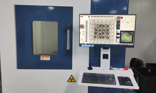
In high-reliability hardware engineering, a design that looks flawless in CAD simulation can still fail catastrophically on the factory floor. Etching chemistry over-etches fine copper traces, solder bridges between adjacent QFN pins during wave soldering, or components collide during automated pick-and-place. Preventing these yield-destroying bottlenecks before committing capital to tooling is the core mission of DFM.
Whether you are launching your first IoT prototype or scaling automotive power electronics to millions of units, understanding what DFM is in manufacturing bridges the gap between theoretical electrical design and practical manufacturing feasibility.
This guide explains what DFM means in engineering, the core principles of design for manufacturing, how DFM compares to DFA, and real-world examples in PCB fabrication and assembly.
Key takeaways
- DFM definition: DFM stands for Design for Manufacturing (or Design for Manufacturability). It is the engineering practice of designing products specifically so they can be produced easily, cost-effectively, and reliably.
- Why DFM is important: Up to 70% of a product's final manufacturing cost and yield is locked in during the initial design phase. DFM catches process conflicts before raw materials are purchased.
- DFM vs DFA: DFM optimizes individual part fabrication (e.g., bare PCB etching, drilling, solder mask registration), whereas DFA (Design for Assembly) optimizes how components fit together during soldering and mechanical box-build.
- Core DFM principles: Standardize materials and component packages, design within verified vendor tolerance envelopes, eliminate tight aspect ratios, and design for testability.
- Actionable PCB examples: Proper annular ring margins, solder mask web dam thickness (minimum 4 mil), copper balance across stackup layers, and thermal reliefs on ground planes.
What is DFM? Meaning and definition in engineering
In engineering and manufacturing, DFM means Design for Manufacturing (or Design for Manufacturability). It represents an integrated methodology where product design and production capability are evaluated concurrently rather than sequentially.
Historically, hardware development operated in silos: design engineers "threw designs over the wall" to factory production teams, who were left to struggle with impossible tolerances, high scrap rates, and delayed lead times. DFM flips this dynamic. By embedding manufacturing process constraints—such as machine tool capabilities, chemical etch tolerances, thermal profiles, and material behavior—directly into the CAD design phase, engineering teams guarantee that what is modeled on screen can be fabricated with high yields.
In modern electronics, dfm manufacturing is not an optional post-design audit; it is a fundamental discipline governing every phase from schematic capture to fabrication drawing sign-off.
What are the key principles of DFM?
While specific rules vary across sheet metal, injection molding, and electronics, five universal dfm principles govern every successful hardware build:
1. Standardization of materials and components
Restricting your Bill of Materials (BOM) to standardized, off-the-shelf laminates (such as standard FR-4 glass styles 1080 and 7628) and preferred passive packages (such as 0402 or 0603 rather than obsolete odd-form parts) shortens procurement cycles, lowers unit costs, and eliminates tooling changeovers on SMT lines.
2. Design within process capability envelopes (Cpk > 1.33)
Every manufacturing step has statistical process variation. A fab shop might specify a nominal minimum trace width of 3 mil, but routing millions of traces at exactly 3 mil pushes the process to its statistical limit. Designing with healthy margins (e.g., 4 or 5 mil wherever space permits) ensures high yields and prevents scrap when etch baths drift. When sizing high-current or thermal conductors, the PCB trace width calculator (IPC-2221) checks that trace geometry satisfies temperature rise limits without violating minimum etching clearances.
3. Minimize complexity and processing steps
Every additional manufacturing operation adds scrap risk and compounding cost. In bare board fab, eliminating unnecessary blind and buried microvias, avoiding sequential lamination cycles unless strictly dictated by routing density, and standardizing hole drill diameters reduces drill bit wear and processing hours.
4. Thermal and mechanical symmetry
In multilayer PCB fabrication, asymmetric copper distribution causes severe board warpage (bow and twist) during lead-free reflow heating ($260^\circ\text{C}$). DFM demands balancing copper area and dielectric thickness symmetrically around the board's center core to maintain planar stability.
5. Design for inspection and testing (DFT)
A board that cannot be tested quickly cannot be manufactured efficiently. DFM dictates placing dedicated test pads (minimum 28–30 mil diameter with 75 mil center-to-center spacing) on all critical nets to support In-Circuit Testing (ICT) and Flying Probe validation without relying on delicate component leads.
DFM vs DFA: Understanding the differences
Engineers frequently combine dfa dfm under the broader umbrella of DFMA (Design for Manufacturing and Assembly), but they address distinct production phases:
| Metric | DFM (Design for Manufacturing) | DFA (Design for Assembly) |
|---|---|---|
| Primary Focus | Fabrication of individual bare parts | Combining parts into higher-level assemblies |
| PCB Application | Bare board etching, lamination, drilling, plating, soldermask | SMT component placement, reflow soldering, wave soldering, THT insertion |
| Typical Goal | Maximize fab yield, prevent shorts/opens, control impedance | Minimize placement errors, prevent solder bridging, eliminate manual solder rework |
| Key Rules | Min trace/space, annular ring, drill-to-copper clearance | Component-to-component clearance, shadow effect avoidance, pin orientation marks |
| Inspection Tool | Bare board electrical test (E-test), cross-section microsectioning | Automated Optical Inspection (AOI), 3D Solder Paste Inspection (SPI), X-ray (AXI) |
Understanding dfm vs dfa ensures teams address both board fabrication limits with the PCB vendor and component placement rules with the SMT assembly provider.
Real-world DFM examples in PCB design
To illustrate how manufacturing dfm works in day-to-day engineering, consider three classic PCB layout scenarios:
Example 1: Annular ring breakout and drill wander
In high-layer-count PCBs, mechanical drill bits wander slightly as they penetrate composite glass-epoxy stacks. If an engineer specifies a via pad diameter of 16 mil with a 10 mil drill hole, the annular ring width is only 3 mil:
$$\text{Annular Ring} = \frac{\text{Pad Diameter} - \text{Drill Diameter}}{2} = \frac{16 - 10}{2} = 3\text{ mil}$$
If the drill wanders by just 2 mil during production, drill breakout occurs, severing the connection between the copper barrel and internal traces. An effective DFM rule requires minimum 4 mil annular rings on outer layers and 5 mil on inner layers for IPC Class 2 reliability, preventing catastrophic opens.
Example 2: Solder mask slivers and solder bridges
When fine-pitch integrated circuits (such as 0.5 mm pitch QFNs or ICs) are placed close together, the solder mask dam between neighboring copper pads must be wide enough to adhere to the substrate. If the solder mask web is less than 3 mil (0.075 mm), the green photoresist lifts during chemical developing, leaving bare copper exposed between pads. During automated reflow, molten solder bridges the gap, creating dead shorts. DFM enforces minimum 3.5–4.0 mil solder mask bridges or mandates Solder Mask Defined (SMD) pad geometries.
Example 3: Thermal relief on large copper planes
Connecting a through-hole component pin directly to a solid internal ground plane creates a massive heatsink. During wave soldering or hand rework, the plane sinks heat away so rapidly that the solder joint fails to reach wetting temperature, resulting in cold solder joints and poor barrel fill. Applying a DFM thermal relief pattern (spoke connections) restricts thermal conduction while maintaining adequate electrical current capacity.
Why is DFM important in modern product development?
Executing formal DFM reviews prior to ordering production boards delivers four measurable financial and engineering dividends:
- Elimination of costly engineering respins: Fixing a footprint mismatch or clearance violation in CAD costs zero dollars. Discovering the defect after assembling 500 boards can cost tens of thousands in scrapped silicon and delayed delivery.
- Shortened time-to-market: Boards designed to factory DFM guidelines pass CAM engineering queries in hours, avoiding protracted Engineering Queries (EQs) that delay fab queues.
- Optimized unit pricing: Designing within standard process tolerances avoids premium tier charges associated with micro-tooling, laser direct imaging, or advanced sequential lamination.
- Predictable long-term field reliability: Eliminating high-stress mechanical points and thin dielectric barriers directly suppresses field failure rates under automotive and industrial thermal cycling.
For detailed design rules, clearance metrics, and drill tolerance matrices, consult APTPCB's comprehensive PCB design for manufacturing guide and online engineering resources.
Frequently Asked Questions
Q: What is DFM in simple terms? A: DFM (Design for Manufacturing) means designing products with the manufacturing process in mind so they can be produced smoothly, with minimal defects, high speed, and the lowest possible scrap cost.
Q: What is the difference between DFM and CAD DRC? A: Design Rule Checking (DRC) in CAD software checks basic geometric rules (such as minimum trace spacing) against predefined software constraints. DFM evaluates how real-world physical processes (chemical etching, plating chemistry, thermal expansion, component shadow effects) behave in actual factory equipment.
Q: When should DFM be conducted during the design process? A: DFM should begin during schematic capture and stackup definition, continue through critical component placement, and conclude with a final CAM verification before Gerber release. Conducting DFM only at the very end often forces painful, time-consuming layout redesigns.
Q: Does DFM compromise product performance? A: No. Proper DFM optimizes performance by ensuring consistent impedance, eliminating parasitic variations from etch undercut, and establishing robust thermal and mechanical reliability.