
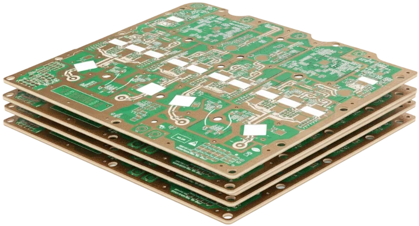
When you look at a bare printed circuit board, the iconic green, matte black, or deep blue protective coating covering the copper surface is the solder mask (also known as solder resist). Without this durable polymer layer, manufacturing modern surface-mount electronics would be virtually impossible.
During high-speed automated wave and reflow soldering, molten solder naturally seeks out any exposed copper. If bare copper traces ran directly beneath components without a barrier, molten solder would wick across conductors, creating disastrous solder bridges and short circuits.
This engineering guide explains what is a solder mask, how solder resist material is applied, compares the major solder mask types and colors, and details the essential DFM design rules for clearances and solder mask dams.
Key takeaways
- What solder mask is: A thin, heat-resistant polymer coating applied over the outer copper layers of a PCB, leaving only component pads and test points exposed.
- Primary functions: Prevents solder bridging during assembly, protects copper from atmospheric oxidation and corrosion, and provides electrical insulation between tightly spaced conductors.
- Main technology: Liquid Photoimageable (LPI) solder mask is the universal industry standard, applied via curtain coating, screen printing, or spray coating, then exposed with UV light or Laser Direct Imaging (LDI).
- Colors and optical inspection: Green remains the industry default because it offers superior visual contrast for inspection, permits the tightest resolution (3.5–4.0 mil dams), and cures most uniformly. Black, white, blue, red, and yellow are widely used for aesthetics, thermal emissivity, or LED reflection.
- Critical DFM rules: Solder mask clearance (typically +2 to +3 mil per side around copper pads) and minimum solder mask web dam thickness (3.5 to 4.0 mil) prevent solder bridging between fine-pitch IC pins.
What is a solder mask? Definition and purpose
In electronics manufacturing, a solder mask (frequently called pcb solder resist or soldermask) is a permanent protective polymer coating applied to the external surfaces of a rigid or flexible circuit board.
The primary functions of solder masking include:
- Preventing solder bridging: Solder mask creates a physical and chemical barrier that prevents molten alloy from spanning the narrow gap between adjacent conductors during wave soldering, selective soldering, or convective reflow.
- Preventing copper oxidation: Bare copper oxidizes rapidly in air, compromising solderability and electrical performance. The mask seals the copper circuitry against humidity, oxygen, dust, and handling contaminants.
- Electrical insulation: Solder mask provides high dielectric breakdown resistance (typically 500 V/mil or > 20 kV/mm), preventing high-voltage arcing between closely spaced traces.
- Restricting solder volume: By isolating SMT pads into discrete openings, the mask prevents solder paste from wicking away from component leads into connecting traces or via holes.
Types of solder mask materials
Several distinct solder mask material formulations are utilized across the industry, categorized by their chemical carrier and application method:
| Solder Mask Type | Application Method | Typical Thickness | Minimum Dam Resolution | Typical Application |
|---|---|---|---|---|
| Liquid Photoimageable (LPI) | Curtain coat / Spray / Screen print + UV / LDI | 0.8–1.2 mil (20–30 µm) | 3.5–4.0 mil (90–100 µm) | Industry standard for > 95% of rigid PCBs |
| Dry Film Solder Mask (DFSM) | Vacuum lamination of solid photosensitive sheet | 1.0–3.0 mil (25–75 µm) | 4.0–5.0 mil (100–125 µm) | High-reliability flex PCBs, uniform planar topography |
| Epoxy Liquid Solder Mask | Thermal-cured screen printing | 1.0–2.0 mil (25–50 µm) | 6.0–8.0 mil (150–200 µm) | Low-cost consumer boards, simple 1–2 layer boards |
| Top-Coating / Peelable Mask | Screen printed temporary synthetic rubber | 10–20 mil (250–500 µm) | N/A (Manual peel) | Temporary protection of gold fingers during wave soldering |
Why LPI dominates the industry
LPI solder mask (Liquid Photoimageable) represents the overwhelming industry choice because liquid polymers flow seamlessly into the recesses between fine copper traces, eliminating air entrapment. Once dried to a tack-free state, the panel is exposed to precision UV light through photographic artwork or direct laser imaging (LDI), followed by chemical development in an aqueous sodium carbonate bath. Only the unexposed pads are washed away, leaving razor-sharp aperture edges.
PCB solder mask colors: Green, black, blue, and beyond
Why is the green solder mask so ubiquitous, and why do designers choose alternative colors?
| Color | Contrast for AOI / Inspection | Minimum Dam Capability | Gloss / Matte Options | Primary Use Case |
|---|---|---|---|---|
| Green (Standard) | Highest contrast (white silkscreen, copper) | 3.5–4.0 mil (0.09 mm) | Glossy or Matte | Universal default; highest yield and fastest processing |
| Matte Black / Gloss Black | Low (hard to inspect traces) | 4.5–5.0 mil (0.12 mm) | Glossy or Matte | Consumer audio, high-end PC hardware, stealth enclosures |
| Blue | Moderate | 4.0–4.5 mil (0.10 mm) | Glossy | Arduino-style boards, industrial controls |
| Red | High | 4.0–4.5 mil (0.10 mm) | Glossy | SparkFun style, test equipment, red status indicators |
| White | High against silkscreen, low trace visibility | 4.5–5.0 mil (0.12 mm) | High-reflectance | LED lighting fixtures (maximizes lumen reflection) |
| Yellow | High | 4.0–4.5 mil (0.10 mm) | Glossy | High-visibility warning modules, robotics |
| Clear / Transparent | Trace visibility only | 4.0 mil (0.10 mm) | Glossy | Decorative, educational kits, flex circuit prototypes |
Why is the PCB green?
Historically, early US military specifications (such as MIL-PRF-55110) standardized on brown paper-phenolic resins combined with green-tinted epoxy resins. Over time, chemical suppliers optimized green pigments to deliver the highest transparency during UV curing. Furthermore, the human eye is most sensitive to green wavelengths (around 555 nm), reducing eye fatigue during manual inspection and offering the highest optical contrast for Automated Optical Inspection (AOI) cameras.
Solder mask thickness and planar coverage
Standard solder mask thickness varies across the board profile:
- On copper trace surfaces: Typically 0.8 to 1.2 mil (20 to 30 µm).
- On trace knees / corners: Thins slightly to 0.4 to 0.6 mil (10 to 15 µm) due to liquid surface tension.
- Between traces (laminate valleys): Fills the gap up to 1.0 to 1.5 mil (25 to 38 µm).
If solder mask is applied too thin (< 0.4 mil over trace edges), dielectric breakdown risk increases and traces may oxidize. If applied too thick (> 1.5 mil on surface pads), tall solder mask walls prevent flat component seating during SMT placement, causing tombstoning or skewed BGA solder balls.
Critical DFM rules: Clearances, dams, and mask-defined pads
When preparing Gerber files, designers must adhere to three foundational solder mask rules:
1. Solder mask expansion (clearance)
CAD layout tools generate solder mask aperture openings slightly larger than the copper pad to accommodate mechanical registration tolerances. Standard clearance is +2 to +3 mil (0.05 to 0.075 mm) per side (total +4 to +6 mil enlargement over pad diameter). If expansion is zero or negative, misaligned mask encroaches onto the copper pad, shrinking solderable area.
2. Solder mask dam (web thickness)
The sliver of green resist separating two adjacent copper pads is the solder mask dam (or solder web). To adhere reliably without peeling or blistering during wave soldering, green LPI mask requires a minimum dam width of:
- Standard green mask: Minimum 3.5 to 4.0 mil (0.09 to 0.10 mm).
- Black, white, or matte colors: Minimum 4.5 to 5.0 mil (0.11 to 0.125 mm).
If the distance between pads is less than 6 mil, subtracting a 2 mil mask clearance on each pad leaves only a 2 mil dam, which will flake off during chemical development. In such cases, designers must switch to a "gang mask" relief (one large aperture exposing both pads) or implement Solder Mask Defined pads.
3. SMD vs NSMD pads
- Non-Solder Mask Defined (NSMD): The mask opening is larger than the copper pad, leaving bare substrate around the pad perimeter. Solder wets both the top and sidewalls of the copper pad, providing maximum mechanical anchoring and predictable impedance. NSMD is strongly recommended for standard fine-pitch BGAs.
- Solder Mask Defined (SMD): The mask opening is smaller than the copper pad, overlapping the edges. This stabilizes fragile ultra-fine pads against peeling under heavy mechanical shear, but slightly reduces solderable pad area.
The color and finish choices above sit inside a larger fabrication spec — our printed circuit board fabrication overview lists the stackup and finish options a mask decision combines with.
Frequently Asked Questions
Q: What is the difference between solder mask and silkscreen? A: Solder mask is the permanent polymer coating (usually green) that insulates copper and prevents solder bridges. Silkscreen is the printed ink layer (usually white) applied on top of the cured solder mask to display text, component outlines, polarity indicators, and logos.
Q: Can you solder directly onto solder mask? A: No. Solder mask is a cured thermoset polymer that repels liquid solder. Solder will only wet bare copper areas protected with a surface finish (such as HASL, ENIG, or Immersion Silver).
Q: What happens if a solder mask dam is too thin? A: If a solder mask dam between closely spaced pads is narrower than 3.5 mil, the chemical developer washes it away, or the fragile sliver breaks off during handling. The resulting gap allows molten solder to flow between adjacent pins during reflow, causing electrical shorts.
Q: Does solder mask color affect PCB cost? A: Standard glossy green solder mask is typically offered with zero premium and the fastest turnaround time. Specialized colors such as matte black, pure white, purple, or pink may require a small tooling surcharge or add 24 hours to production lead time due to dedicated cleaning of coating equipment.
Q: Is solder mask waterproof? A: Solder mask is moisture-resistant and protects against atmospheric humidity, but it is not completely hermetic. For outdoor or marine electronics requiring true waterproofing, a secondary conformal coating or potting process is required over the fully assembled PCBA.