
Connectivity
An accessible net is open or shorted
The program can identify the affected test nodes and narrow the repair search when probe access and fixture contact are valid.
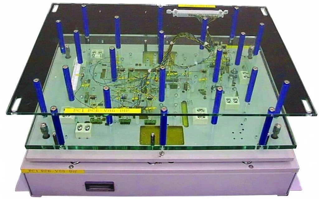
In-Circuit Test Service
Confirm test-point access, component checks, electrical limits, fixture scope, and result fields before tooling is released. APTPCB develops the ICT setup around the approved design data and production test plan.
In-circuit test
| Question | Answer |
|---|---|
| What is in-circuit test? | In-circuit test (ICT) checks individual components, nets and interconnects on an assembled PCBA through a bed-of-nails fixture, before the board is powered up for functional test. |
| When is ICT the right choice? | When the board has probe access on most nets, the quantity justifies a fixture, and you need per-net fault isolation rather than a pass/fail result. |
| What does ICT not cover? | Nets with no probe access, most BGA joints, firmware behaviour and system-level function. Those need boundary scan, X-ray, or FCT. |
Testability decision
In-circuit test needs a physical probe contact on every net it checks. Whether ICT is viable is decided by board geometry, not by the tester. Review these conditions before ordering a fixture, because a board that cannot be probed cannot be rescued by a better program.
| Board condition | ICT viable? | Reason | Alternative |
|---|---|---|---|
| Nets brought out to test pads on one or both sides | Yes | Standard bed-of-nails access; fixture can be built from the CAD data | — |
| Test pads present, but tall components on the probe side | Yes, with a custom fixture | Probe side needs relief cut-outs and board support to avoid flex | Selective or dedicated fixture |
| BGA nets with no via or test pad escape | No — not physically probeable | There is no contact point under the package for a needle | Boundary scan, X-ray, or FCT coverage |
| Bottom-terminated packages (LGA, QFN) on the probe side | Partly | Only exposed perimeter pads are reachable; the centre terminator is not | AOI plus boundary scan |
| Fine pitch below roughly 0.3 mm | Possible but costly | Probe and fixture tolerance drive cost and maintenance sharply | Flying probe |
| High-current or high-voltage nets | Yes, with isolation | Probes and guarding must be rated for the net, or readings mislead | FCT with dedicated loads |
| Very low-volume or prototype builds | Usually not justified | Fixture and program cost is not recovered across a small quantity | Flying probe or FCT |
ICT coverage is limited by access, not by intent. Where coverage is impossible, that boundary is stated in the test plan rather than implied as full coverage.
Coverage matrix
The approved design data and limits define which checks are practical. This matrix separates common ICT targets from the inputs and boundaries that must be confirmed for the actual assembly.
| Test target | Typical ICT check | Required baseline | Important boundary |
|---|---|---|---|
| Nets and interconnects | Continuity, opens, unintended shorts, and selected node-to-node relationships | Netlist or CAD data, accessible test points, and approved connectivity | A net without practical probe or boundary-scan access may remain uncovered |
| Resistors | Value or range checks where the surrounding circuit permits isolation | BOM value, tolerance, reference designator, and circuit context | Parallel paths can affect the measured value and may require guarding or exclusion |
| Capacitors and inductors | Presence and selected value or impedance checks where measurable | Nominal value, tolerance, package, and approved test method | Small values, parallel networks, and charged nodes can limit useful coverage |
| Diodes and transistors | Junction orientation, forward response, and selected device checks | Device type, pin mapping, expected response, and safe stimulus limits | In-circuit paths and device protection can constrain the available measurement |
| IC power and accessible pins | Power-to-ground relationships, pin connections, and boundary-scan checks where supported | Schematic, package pinout, safe power conditions, and boundary-scan data if used | ICT does not automatically verify internal IC behavior or firmware operation |
| Connectors and test interfaces | Accessible pin continuity, isolation, and defined fixture connections | Connector pin map, mating or fixture method, mechanical access, and limits | Mechanical fit and powered interface behavior may require separate inspection or FCT |
A listed component or net is not automatic coverage. The released coverage report should identify tested, conditionally tested, boundary-scan, and uncovered items for the approved design revision.
Electrical defect isolation
ICT complements assembly inspection by checking accessible electrical relationships against the released program and design-specific limits.
The program can identify the affected test nodes and narrow the repair search when probe access and fixture contact are valid.
A value outside the approved range can indicate a wrong part, placement mix-up, damaged device, or circuit condition that needs review.
Junction response and pin relationships can expose selected orientation errors when the surrounding circuit permits a reliable check.
Board- or lot-linked failure codes can support repair disposition and trend review without claiming that ICT alone proves the root cause.
Test-method selection
These methods answer different questions. The production test strategy can combine them when visual defects, hidden joints, accessible nodes, and powered product behavior all matter.
| Method | Best fit | What it primarily checks | Important boundary |
|---|---|---|---|
| Flying probe | Prototype, NPI, lower volume, or designs not yet ready for dedicated tooling | Accessible nets and selected component relationships with flexible probe movement | Typically trades cycle time for lower fixture commitment and easier program changes |
| ICT | Stable designs and repeat production where dedicated tooling is justified | Repeatable checks of accessible nets, shorts, opens, and selected components | Coverage depends on test access, circuit isolation, fixture quality, and released limits |
| AOI and X-ray | Visible workmanship and defined hidden-joint inspection | Placement, polarity, solder features, and internal assembly features within scope | Inspection images do not prove electrical continuity or product behavior |
| FCT | Powered operation against approved firmware, stimuli, interfaces, and loads | Product-specific responses, sequences, measurements, and functional limits | ICT does not prove complete product behavior, so FCT may still be required |
Use the PCBA testing and quality hub to map methods to design maturity, accessible test points, expected volume, failure risk, and required evidence.
Design review to production release
Each gate closes a source of missed defects, false failures, fixture damage, or untraceable results before ICT is used for production release.
Action: align the CAD or netlist, schematic, BOM, revision, test points, and boundary-scan files. Risk: tooling against incomplete or mismatched data. Evidence: reviewed input package and open-access list.
Action: define probe locations, support pins, clamping, keep-outs, connectors, and safe contact force. Risk: unstable contact, board flex, component interference, or damage. Evidence: released fixture definition and ownership terms.
Action: map tests, stimuli, isolation or guarding methods, nominal values, tolerances, and fault messages. Risk: limits that do not match the circuit or component tolerance. Evidence: versioned program and draft coverage report.
Action: run approved pilot boards, review contact stability, challenge known conditions, and tune justified limits. Risk: false rejects or unrecognized coverage gaps. Evidence: pilot results, approved exceptions, and golden-board or reference method.
Action: release the fixture, probe map, program, limits, work instruction, and repair and retest flow. Risk: design or BOM changes invalidating the baseline. Evidence: controlled revision and board- or lot-linked records as ordered.
In-circuit test planning
Records and RFQ closure
A pass label without revision control or a coverage boundary is weak production evidence. Agree the tested scope, identity fields, failure detail, retention, and disposition flow needed by engineering, quality, and procurement.
Send the design revision, CAD or netlist, schematic, BOM, test-point list, component references, electrical limits, boundary-scan package where applicable, board-support constraints, quantity forecast, serialization method, and required report fields.
ICT verifies only the accessible checks included in the released program. It does not prove firmware-driven operation, product performance under real loads, complete solder-joint quality, regulatory compliance, or system qualification.
| Record field | Purpose |
|---|---|
| Board or lot identity | Connect the ICT result to the agreed serial number or lot method |
| Design and program revision | Show which approved hardware data, limits, and test program applied |
| Pass/fail and failed node | Support fault isolation and disposition with the available test detail |
| Measured value and limit | Retain parametric evidence where the released ICT program records it |
| Repair and retest status | Close the nonconforming-board flow under the agreed order procedure |
Coverage-report format, measured values, sampling, retention, and serialization depend on the released program and order.
Confirm fixture ownership, revision and maintenance terms, spare probes or wear items, expected volume, change-control triggers, coverage-report format, pilot acceptance, and the repair and retest path.
Send the available CAD or netlist, schematic, BOM, test-point information, electrical limits, boundary-scan package, expected volume, and reporting needs. We will confirm practical coverage and quote assumptions before tooling release.