
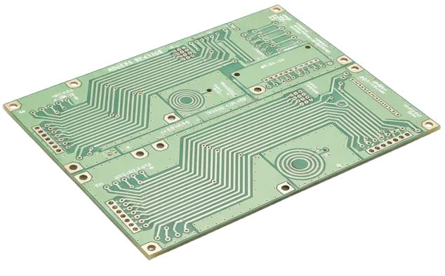
High-frequency RF and microwave architectures operating from sub-6 GHz telecom bands up to 77 GHz automotive radar arrays face a persistent engineering conflict: pure high-frequency laminates (such as PTFE composites or ceramic-filled hydrocarbons) provide minimal dielectric dissipation ($Df < 0.003$), but building an entire 8- to 16-layer stackup purely from these microwave materials increases raw substrate costs by 400% to 800% while exacerbating Z-axis thermal expansion risks during lead-free assembly.
Hybrid mixed-dielectric lamination resolves this conflict by restricting low-loss microwave laminates to critical outer signal layers carrying microstrips, coplanar waveguides, and antennas, while standard high-$Tg$ FR-4 cores manage internal baseband routing, power delivery, and ground distribution. Successfully executing a hybrid build requires matching resin cure kinetics, balancing thermal expansion to prevent post-lamination bow and twist, and selecting copper surface profiles that prevent skin-effect conductor losses from dominating the microwave transmission budget.
| Substrate Category | Typical Laminate | Dielectric Constant ($Dk$ at 10 GHz) | Dissipation Factor ($Df$ at 10 GHz) | Z-Axis CTE ($50^\circ\text{C} - 260^\circ\text{C}$) | Autoclave Lamination Window | Typical Application Layer in Hybrid Stack |
|---|---|---|---|---|---|---|
| Standard FR-4 | Standard Epoxy / E-Glass | $4.4 - 4.6$ | $0.018 - 0.022$ | $60 - 85\text{ ppm/}^\circ\text{C}$ | $170^\circ\text{C} - 180^\circ\text{C}$ | Internal DC power and low-speed digital buses |
| High-$Tg$ FR-4 | Isola 370HR / S1000-2M | $3.92 - 4.04$ | $0.015 - 0.018$ | $45 - 55\text{ ppm/}^\circ\text{C}$ | $175^\circ\text{C} - 185^\circ\text{C}$ | Internal high-speed digital and structural core |
| Ceramic Hydrocarbon | Rogers RO4350B / RO4003C | $3.48 \pm 0.05$ | $0.0037$ | $32\text{ ppm/}^\circ\text{C}$ | $175^\circ\text{C}$ (Standard FR-4 cycle) | Outer RF microstrips, matching networks, antennas |
| Thermoset RF Bondply | Rogers RO4450F / RO4450T | $3.52 \pm 0.05$ | $0.0040$ | $40\text{ ppm/}^\circ\text{C}$ | $175^\circ\text{C} - 180^\circ\text{C}$ | Mixed dielectric interface bond layer |
| PTFE Composite | Rogers RO3003 / RT/duroid | $3.00 \pm 0.04$ | $0.0010$ | $24\text{ ppm/}^\circ\text{C}$ | $360^\circ\text{C}$ fusion or specialized bond film | High-frequency 77 GHz radar sensors & phased arrays |
High-Frequency Dielectric Physics: Dispersion, Loss Tangent, and Skin Depth
At direct current (DC) and low frequencies, electrical signals travel through the entire cross-sectional volume of a copper trace. As frequency climbs into the gigahertz spectrum, two electromagnetic phenomena dominate PCB performance: Dielectric Dissipation ($Df$) and the Skin Effect ($\delta$).
                           ELECTROMAGNETIC ATTENUATION REGIMES
                           ===================================
                           Total Attenuation α_total = α_d + α_c

    Dielectric Loss (α_d): Dominates by substrate Df    Conductor Loss (α_c): Dominates by skin depth &
    α_d ≈ 2.3 x f x √Dk x tan(δ)  [dB/in]               surface roughness R_z
1. The Skin Depth Calculation
Due to eddy currents induced within the conductor, alternating current concentrates exponentially at the outer periphery of the copper trace. The skin depth ($\delta$) represents the depth below the surface where current density drops to $1/e$ ($36.8%$):
$$\delta = \sqrt{\frac{\rho}{\pi \cdot f \cdot \mu_0 \cdot \mu_r}} = \frac{66.1}{\sqrt{f}} \quad (\mu\text{m, for standard copper at } 20^\circ\text{C})$$
Where:
- $\rho = 1.72 \times 10^{-8}\ \Omega\cdot\text{m}$ (resistivity of annealed copper)
- $\mu_0 = 4\pi \times 10^{-7}\ \text{H/m}$ (permeability of free space)
- $\mu_r = 1.0$ (relative permeability of copper; non-magnetic)
- $f$ is frequency in Hertz
       Skin Depth vs. Operating Frequency in Pure Copper:
       - At 1 GHz:    δ = 2.09 µm
       - At 5.8 GHz:  δ = 0.87 µm
       - At 10 GHz:   δ = 0.66 µm
       - At 28 GHz:   δ = 0.39 µm (5G mmWave Band)
       - At 77 GHz:   δ = 0.24 µm (Automotive Radar Band)
At $28\text{ GHz}$, all RF current flows through a microscopic outer skin only $0.39\ \mu\text{m}$ deep. If the copper foil possesses a standard dendritic tooth roughness ($R_z \approx 4 - 7\ \mu\text{m}$), the electromagnetic wave is forced to travel along the tortuous valleys and peaks of the copper teeth, drastically lengthening the effective physical path and increasing conductor loss by $30% - 50%$.
High-Frequency Dielectric Substrate Material Matrix
Selecting the proper core material requires balancing high-frequency dielectric stability against thermal-mechanical compatibility with FR-4 manufacturing lines.
| Substrate Material Family | Resin / Reinforcement Chemistry | Dielectric Constant ($Dk$ at $10\text{ GHz}$) | Dissipation Factor ($Df$ at $10\text{ GHz}$) | Thermal Conductivity ($k$ in $\text{W/m}\cdot\text{K}$) | Z-Axis CTE ($50^\circ\text{C} - 260^\circ\text{C}$) | Moisture Absorption | Relative Material Cost Multiplier |
|---|---|---|---|---|---|---|---|
| Standard FR-4 | Difunctional Epoxy / E-Glass | $4.4 - 4.6$ | $0.018 - 0.022$ (Very High Loss) | $0.25 - 0.30$ | $60 - 85\text{ ppm/}^\circ\text{C}$ | $0.35% - 0.50%$ | $1.0\times$ (Baseline) |
| High-$Tg$ FR-4 (Isola 370HR) | Multifunctional Epoxy / E-Glass | $3.92 - 4.04$ | $0.015 - 0.018$ | $0.40 - 0.50$ | $45 - 55\text{ ppm/}^\circ\text{C}$ | $0.15% - 0.25%$ | $1.3\times - 1.6\times$ |
| Panasonic Megtron 6 | Low-Loss Polyphenylene Oxide (PPO) | $3.40 - 3.60$ | $0.002 - 0.004$ (Ultra Low) | $0.40 - 0.45$ | $38 - 45\text{ ppm/}^\circ\text{C}$ | $0.05% - 0.10%$ | $3.5\times - 4.5\times$ |
| Rogers RO4003C | Ceramic-Filled Hydrocarbon / Woven Glass | $3.38 \pm 0.05$ | $\mathbf{0.0027}$ | $0.71$ (High Thermal) | $46\text{ ppm/}^\circ\text{C}$ | $0.04%$ | $4.0\times - 5.5\times$ |
| Rogers RO4350B | Ceramic-Filled Hydrocarbon (UL 94V-0) | $3.48 \pm 0.05$ | $\mathbf{0.0037}$ | $0.69$ | $32\text{ ppm/}^\circ\text{C}$ (Matched to Cu) | $0.04%$ | $4.5\times - 6.0\times$ |
| Rogers RO3003 | Ceramic-Filled PTFE (Unwoven Glass) | $3.00 \pm 0.04$ | $\mathbf{0.0010}$ (Extremely Low) | $0.50$ | $24\text{ ppm/}^\circ\text{C}$ | $0.04%$ | $6.0\times - 8.5\times$ |
| Taconic TLY-5 | Pure PTFE / Woven Glass Microfiber | $2.20 \pm 0.02$ | $\mathbf{0.0009}$ | $0.22$ | $130\text{ ppm/}^\circ\text{C}$ (High Expansion) | $0.02%$ | $7.0\times - 10.0\times$ |
[!IMPORTANT] Why RO4350B is the Preferred Hybrid Core: Rogers RO4350B is a thermoset material that processes exactly like standard FR-4: it requires no specialized plasma desmear or sodium etching for plated through-holes, withstands standard multi-opening vacuum lamination press cycles, and meets UL 94V-0 flame-retardancy standards without halogenated additives.
Hybrid Stackup Architecture & Mixed-Lamination Rules
When lamination combines substrates with differing moduli of elasticity and coefficients of thermal expansion, severe mechanical warpage (bow and twist exceeding $0.75%$ under IPC-TM-650 2.4.22) can occur unless the stackup is strictly balanced.
                  6-LAYER SYMMETRICAL RF HYBRID STACKUP
                  =====================================
    Layer 1: TOP RF Signal ─────────────── Microstrip / Antennas (RO4350B, 18 µm VLP Copper)
    Dielectric 1-2: 0.508 mm (20 mil) Rogers RO4350B Core (Dk = 3.48, Df = 0.0037)
    Layer 2: RF Ground Plane ───────────── Solid RF Reference Ground (18 µm VLP Copper)
    Dielectric 2-3: 2x 1080 Rogers RO4450F Thermoset Bondply (Curing Temp: 175°C)
    Layer 3: Digital Power Plane ──────── Solid DC Power Distribution (35 µm Copper)
    Dielectric 3-4: 0.40 mm High-Tg FR-4 Core (Isola 370HR, Tg = 180°C)
    Layer 4: High-Speed Digital Bus ───── Digital Control / SPI / I2C Traces
    Dielectric 4-5: 2x 1080 Rogers RO4450F Bondply
    Layer 5: Digital Ground Plane ─────── Secondary Ground Reference
    Dielectric 5-6: 0.508 mm Rogers RO4350B Core (Mechanical Warpage Balance)
    Layer 6: BOTTOM RF Signal ──────────── Baseband / Power Routing
Core Rules for Mixed-Dielectric Lamination:
- Bondply Selection: Never use standard FR-4 prepreg directly against a ceramic hydrocarbon or PTFE core on critical RF transmission lines. The higher loss tangent of FR-4 prepreg ($Df \approx 0.018$) degrades signal attenuation on the adjacent reference layer. Specify Rogers RO4450F or RO4450T bondply, which shares the identical dielectric chemistry ($Dk = 3.52, Df = 0.004$) and cures at $175^\circ\text{C}$, matching FR-4 autoclave thermal profiles.
- Symmetrical Balance to Prevent Bow & Twist: While placing the RF laminate only on Layer 1 saves cost, an asymmetrical build (e.g., Rogers on top, FR-4 on bottom) creates bimetallic thermal bowing during reflow soldering ($260^\circ\text{C}$) due to the differential shrinkage rates of the resin matrices. For precision boards, mirror the outer dielectric core thickness on the bottom layer.
- Plated Through-Hole Desmear Protocol:
- For Hydrocarbon Ceramic (RO4000 series): Standard permanganate chemical desmear is fully compatible.
- For Pure PTFE Laminates (RO3000 / RT/duroid): Permanganate cannot etch PTFE resin. The board must undergo Plasma Desmear ($80%\ \text{CF}_4 / 20%\ \text{O}_2$ gas mixture) or chemical sodium naphthalene treatment to wet and functionalize the fluoropolymer hole walls prior to electroless copper seed deposition.
Copper Foil Surface Roughness & Insertion Loss Sizing
At microwave frequencies, the physical profile of the copper-dielectric interface dictates conductor attenuation. PCB copper foils are classified by their 10-point mean surface roughness ($R_z$):
       Standard Electrodeposited (STD) Foil       Very Low Profile (VLP) / Rolled Annealed (RA)
       ====================================       =============================================
       ▲  /\  /\      /\    /\  /\  (Rz > 5.0 µm)  ─-─-──-──-─-──-──-─-──-──-─-──-─ (Rz < 1.0 µm)
       │ /  \/  \    /  \  /  \/  \               ─────────────────────────────────────────────
       ▼/        \  /    \/        \              Smooth planar surface: Skin current flows along
       Dendritic tooth anchors force RF current   a direct linear path with minimal ohmic loss.
       into a tortuous, high-resistance path.
Conductor Loss Multiplication Under Cannonball-Huray Physics
| Copper Foil Treatment Class | Average Roughness ($R_z$) | Effective Skin Depth Path Factor | Insertion Loss Penalty at $10\text{ GHz}$ | Insertion Loss Penalty at $28\text{ GHz}$ | Recommended Application Spectrum |
|---|---|---|---|---|---|
| Standard Electrodeposited (STD) | $4.5\ \mu\text{m} - 7.5\ \mu\text{m}$ | $1.40\times - 1.65\times$ | $+25% - 35%$ | $+50% - 70%$ (Severe Loss) | DC power, low-speed digital only |
| Reverse-Treated Foil (RTF) | $2.5\ \mu\text{m} - 3.5\ \mu\text{m}$ | $1.20\times - 1.35\times$ | $+15% - 20%$ | $+30% - 40%$ | Sub-6 GHz cellular, Wi-Fi 6E |
| Very Low Profile (VLP) | $1.2\ \mu\text{m} - 2.0\ \mu\text{m}$ | $1.08\times - 1.15\times$ | $+5% - 10%$ | $+15% - 20%$ | 10 GHz - 24 GHz Radar, 5G NR |
| Hyper-Very Low Profile (HVLP) | $0.6\ \mu\text{m} - 1.0\ \mu\text{m}$ | $1.02\times - 1.05\times$ | $< 3%$ | $+5% - 8%$ | 28 GHz - 40 GHz mmWave front-ends |
| Rolled Annealed (RA) Copper | $\le 0.5\ \mu\text{m} - 0.8\ \mu\text{m}$ | $1.00\times$ (Near Ideal) | Baseline ($0%$) | Baseline ($0%$) | 77 GHz Automotive Radar, Satcom |
DFM Specification: On fabrication prints for high-frequency precision rigid PCBs, explicitly state:"All Layer 1 and Layer 2 copper foils must be specified as IPC-4562 Grade 3 (VLP) or Grade 8 (HVLP) with certified surface roughness Rz <= 1.5 µm."
Passive Intermodulation (PIM) Mitigation in High-Power RF
Passive Intermodulation (PIM) is the generation of unwanted spurious harmonic signals caused by non-linear mixing of two or more high-power transmit carrier frequencies ($f_1, f_2$). In cellular base stations and phased-array radar, these passive intermodulation products (such as third-order $2f_1 - f_2$) fall directly into the receiver band, blinding the front-end low-noise amplifier (LNA).
       Transmitted High-Power Carriers             Generated 3rd-Order Intermodulation (IM3)
       ===============================             =========================================
            (Carrier f1)     (Carrier f2)                     (PIM Product: 2f1 - f2)
                 │                │                                      │
                 │   +43 dBm      │   +43 dBm                            │
                 │   (20 W)       │   (20 W)                             ▼ Falls into RX Band!
                 │                │                               ┌──────────────┐
                 ▼                ▼                               │ < -160 dBc   │ (Target Spec)
       ───────────────────────────────────────────────────────────┴──────────────┴──────────►
                                     Frequency (MHz)
Critical DFM Rules for PIM Suppression ($\le -160\text{ dBc}$):
- Ban Ferromagnetic Nickel in RF Paths: Nickel is a ferromagnetic transition metal. The magnetic hysteresis of nickel creates severe non-linear resistance under high RF currents. Standard Electroless Nickel Immersion Gold (ENIG) generates catastrophic PIM levels ($>-90\text{ dBc}$ to $-110\text{ dBc}$), failing cellular carrier acceptance standards.
- Specify Non-Magnetic Surface Finishes:
- Immersion Silver (IAg): Pure silver is completely non-magnetic, highly conductive ($\sigma = 6.3 \times 10^7\ \text{S/m}$), and provides the lowest PIM performance ($\le -165\text{ dBc}$).
- Immersion Tin (ISn): Excellent non-magnetic performance for automotive radar sensors.
- Direct Immersion Gold (DIG) / ENEPIG with Non-Magnetic Barrier: Solderable and wire-bondable without magnetic distortion.
- Eliminate Micro-Etch Whiskers: Chemical etching must be tightly controlled to prevent micro-protrusions and sharp undercut serrations at trace edges. Sharp conductor points create non-linear microscopic cold-field electron emission under high RF voltages.
RF DFM, Ground Via Fencing, and Solder Mask Keepouts
Designing transmission lines on hybrid RF substrates requires strict physical layout discipline to prevent substrate radiation modes and parasitic phase shifting.
       COPLANAR WAVEGUIDE WITH GROUND (CPWG) & VIA FENCE
       =================================================
       ──[ Ground Plane ]──    ──[ RF Conductor (W) ]──    ──[ Ground Plane ]──
         ○     ○     ○            (Gap S)      (Gap S)       ○     ○     ○
         │     │     │                                       │     │     │  <- Ground Vias
       ════════════════════════════════════════════════════════════════════════  <- RF Ground Plane
       - Pitch between via centers: P <= λ_g / 10 (Suppresses parallel plate radiation)
       - Distance from conductor to via fence: D ≈ 1.5 x W (Prevents modal distortion)
1. Ground Via Fence Stitching Rules
To suppress electromagnetic energy from leaking into the substrate cavity as parallel-plate waveguide modes, ground vias must border both sides of the transmission line:
- Pitch Spacing ($P$): The center-to-center distance between adjacent ground vias must be less than one-tenth of the guided wavelength at the highest operational frequency: $$P \le \frac{\lambda_g}{10} = \frac{c}{10 \cdot f \cdot \sqrt{Dk}}$$ Example: At $28\text{ GHz}$ in RO4350B ($Dk = 3.48$), $\lambda_g \approx 5.74\text{ mm}$. Maximum via pitch is $P \le 0.57\text{ mm}$ ($22\text{ mil}$).
- Conductor Clearance: Maintain a lateral spacing of at least $1.5\times$ to $2\times$ the trace width between the trace edge and the ground via barrel edge to prevent capacitive impedance pulling.
2. Solder Mask Stripping Over RF Microstrips
Standard Liquid Photoimageable (LPI) solder mask is engineered for insulation, chemical resistance, and solder dam containment—not RF propagation:
- Solder mask exhibits a high dissipation factor ($Df \approx 0.02 - 0.035$) and high dielectric constant ($Dk \approx 3.8 - 4.2$).
- Applying solder mask over an RF microstrip trace slows phase velocity, shifts center resonant frequencies by up to $3% - 5%$, and increases dielectric loss by $0.3\text{ dB} - 0.8\text{ dB}$ per inch at $10\text{ GHz}$.
- Mandate: Create an explicit solder mask clearance aperture (
.GTSlayer) covering all high-frequency microstrip lines, matching networks, and planar antenna elements, leaving the copper protected solely by Immersion Silver or Immersion Gold.
High-Frequency RF CAM & Fabrication Release Protocol
Before finalizing CAM engineering and releasing high-frequency hybrid data packages for manufacturing, verify every fabrication parameter against the following engineering release protocol:
| RF Engineering Parameter | Target Specification & Rule | Fabrication Release Verification |
|---|---|---|
| RF Core Laminate by MPN | Rogers RO4350B or RO4003C specified explicitly with core thickness tolerance | Material callout note on drill & fabrication drawing; generic substitutions barred |
| Interface Bondply Material | Rogers RO4450F or RO4450T thermoset bondply matched to FR-4 autoclave cycle | Stackup BOM cross-check; standard FR-4 prepreg prohibited on RF reference interfaces |
| Copper Foil Roughness | Very Low Profile (VLP) or Hyper-VLP ($R_z \le 1.5\ \mu\text{m}$) on RF conductor layers | Mill certificate verification; surface roughness profilometry test report |
| Stackup Symmetrical Balance | Dielectric thickness and copper distribution mirrored across stackup center | Pre-lamination lay-up audit to guarantee bow and twist $\le 0.75%$ |
| Non-Magnetic Surface Finish | Immersion Silver (IAg) or non-magnetic ENEPIG; nickel-based ENIG barred from RF paths | Plating specification drawing; PIM verification testing ($\le -160\text{ dBc}$) |
| Solder Mask Relief Clearance | Mask apertures stripped completely from microstrips, coplanar wave guides, and patch arrays | Gerber .GTS / .GBS overlay inspection against RF conductor layers |
| Via Fence Pitch & Clearance | Ground via spacing $P \le \lambda_g / 10$; conductor-to-barrel edge clearance $\ge 1.5 \times W$ | Automated DRC clearance audit on ground stitching nets |
| Controlled Impedance Modeling | $50\ \Omega$ single-ended ($\pm 5%$) and $100\ \Omega$ differential ($\pm 7%$) coupons defined | TDR coupon test coupon layout on production master panel |
For advanced stackup simulations, complex microvia integration, or precision heavy power routing across RF hybrids, upload your ODB++ or Gerber data directly to our engineering desk at the APTPCB Rigid PCB Manufacturing Portal. For dynamic flexing and gimbal interconnects, explore our Rigid-Flex PCB Dynamic Bend Radius Guide.
High-Frequency Hybrid PCB Stackup & RF FAQs
1. What is the primary advantage of a hybrid Rogers and FR-4 PCB stackup?
A hybrid PCB stackup delivers the electrical performance of high-frequency microwave laminates on critical RF signal layers while using low-cost high-$Tg$ FR-4 for non-RF digital and power routing. This mixed-dielectric approach reduces raw material costs by $50%$ to $70%$ compared to an all-Rogers board, improves mechanical stiffness, reduces Z-axis thermal expansion (protecting plated through-holes from barrel cracking), and enables compatibility with standard multilayer PCB fabrication lines.
2. Can standard FR-4 prepreg be used to laminate Rogers RO4000 series cores?
No, standard FR-4 prepreg should not be used in direct contact with RF microstrip lines or high-speed transmission layers. Standard FR-4 epoxy has a high dissipation factor ($Df \approx 0.018 - 0.022$), which causes severe dielectric loss and phase distortion on adjacent RF reference planes. Resin flow in FR-4 prepreg can also vary laminate thickness and shift controlled impedance. Instead, designers must use specialized thermoset bondply materials such as Rogers RO4450F or RO4450T, which have low loss ($Df = 0.004$) and cure at standard FR-4 autoclave temperatures ($175^\circ\text{C}$).
3. Why does standard ENIG surface finish degrade RF performance and cause PIM?
Electroless Nickel Immersion Gold (ENIG) deposits a layer of electroless nickel ($3 - 6\ \mu\text{m}$) beneath a thin flash of immersion gold. Nickel is a ferromagnetic material with high magnetic permeability ($\mu_r \approx 100 - 600$). In high-frequency alternating electromagnetic fields, nickel's magnetic hysteresis introduces high insertion loss and produces non-linear resistance under high power, generating severe Passive Intermodulation (PIM) distortion ($>-90\text{ dBc}$). For RF and microwave designs, non-magnetic finishes such as Immersion Silver (IAg) or Immersion Tin (ISn) must be specified.
4. How does copper surface roughness affect insertion loss at frequencies above 10 GHz?
At microwave frequencies, current flow is confined to the microscopic outer skin depth of the conductor ($\delta = 0.66\ \mu\text{m}$ at $10\text{ GHz}$; $\delta = 0.39\ \mu\text{m}$ at $28\text{ GHz}$). If the copper foil has standard dendritic tooth roughness ($R_z > 5\ \mu\text{m}$), the current is forced to travel along the undulating microscopic contours of the copper teeth rather than in a straight line. This increases the effective physical distance traveled, increasing conductor resistance and multiplying high-frequency insertion loss by $30%$ to $60%$. Using Very Low Profile (VLP) or rolled-annealed foils ($R_z \le 1.0\ \mu\text{m}$) restores ideal planar transmission efficiency.
5. Why should solder mask be stripped from high-frequency microstrip lines?
Standard Liquid Photoimageable (LPI) solder mask is an uncalibrated dielectric material with a high dielectric constant ($Dk \approx 4.0$) and high dissipation factor ($Df \approx 0.02 - 0.035$). When solder mask coats an RF microstrip trace, the electromagnetic fringe field penetrates the lossy mask, adding $0.3\text{ dB}$ to $0.8\text{ dB}$ of insertion loss per inch at $10\text{ GHz}$. Manufacturing tolerances in solder mask wet coating thickness ($\pm 10\ \mu\text{m}$) also introduce unpredictable impedance shifts and detune resonant RF filters and antenna elements.