
A gold-colored PCB pad is not necessarily a durable plug-in contact. Gold fingers are the conductive contacts along a board edge that mate with a card-edge socket. Their finish, usable contact length, board thickness and lead-in geometry must work together with the selected socket. For repeated mating, use the connector manufacturer's specified contact finish; hardened electroplated gold over nickel is a common requirement, while a solderable immersion-gold finish is not an automatic substitute.
A board can pass electrical continuity testing and still fail to engage its socket correctly. Conversely, a card that slides into a connector may have the wrong contact finish for the intended service life. Release the electrical, mechanical and wear requirements together.
For the general drawing package, see fabrication drawing essentials. For soldered terminal connections, see through-hole soldering basics. Solder-joint acceptance and sliding-contact wear require different evidence.
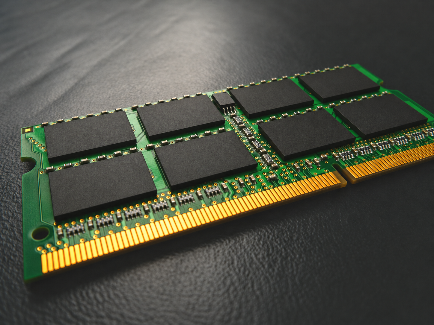
Photo: Franck V. / Unsplash. AI-edited to remove chip-brand markings; some components and surface details may have been reconstructed. Illustrative background only; it cannot establish plating, actual dimensions, service life, or manufacturing results.
What should be decided before choosing the gold finish?
Start with the exact mating connector and its current application drawing. Identify the accepted card thickness, contact pattern, insertion depth, keying, lead-in requirements and finish recommendations. Record how often the card will be installed, whether field replacement is expected and what environment the contact must tolerate. These inputs establish the use case; they do not independently certify a plating stack.
Separate normal service mating from manufacturing handling. A module installed once in the product may still be plugged into several fixtures during programming and test. Count those planned operations when discussing durability with the connector supplier. Avoid converting a broad phrase such as “maintenance access” into an arbitrary number of guaranteed cycles.
Samtec's Connector Plating FAQs recommends hardened gold on mating PCB pads for repeated edge-card use. That supports treating wear resistance as a specific requirement. It does not mean one gold thickness or hardness is correct for every connector family.
Ask which specification controls if a socket drawing, system drawing and procurement note disagree. A fabricator should not have to choose between a contact drawing that requests hard gold and an order form that selects ENIG for the entire board.
Hard gold, ENIG and flash gold are different purchasing descriptions
Electroplated hard gold is intended to provide a wear-resistant contact surface. ENIG describes electroless nickel immersion gold, widely used on soldering lands. Both can look gold, but their deposition processes and intended functions differ. Specify the actual finish system and required properties rather than accepting color as evidence of equivalence.
“Flash gold” is especially incomplete as an order instruction. Ask what deposition process, composition and thickness the supplier means, and whether that condition meets the connector's requirements. The word alone does not define a qualified wear surface. Likewise, the connector's own gold-plated socket contacts do not prove that any gold-colored PCB finish is a compatible mating surface.
A board can require selective hard gold on its contact band and another finish on component soldering lands. Mark the boundaries on the fabrication drawing. Keep the required contact zone distinct from nearby solderable copper, test lands and cosmetic areas; otherwise a quotation may price a different finish area from the one the design needs.
| Drawing region | Requirement to establish | Evidence that answers it |
|---|---|---|
| Sliding contact band | Finish system, nickel and gold requirements, applicable thickness definition and allowed surface condition | Agreed plating measurements and contact-area inspection |
| Component soldering lands | Finish appropriate to the specified assembly process | Identified finish and applicable solderability evidence |
| Insertion edge and lead-in | Finished profile, thickness and relationship to the contact band | Dimensional inspection against the released mechanical drawing |
A single statement such as “gold-plated PCB” leaves all three regions ambiguous. A certificate naming a finish also does not necessarily identify where its thickness was measured. Agree measurement locations, sampling and acceptance before treating a report as release evidence.
A drawing note that keeps finish and evidence together
The following is an organizational example, not a universal plating specification:
Identify the sliding contact region as C1 on both board faces. Apply selective electroplated hard gold over nickel to C1, to the composition, hardness, thickness definition and surface-condition requirements in the released connector-interface specification. Record that document's identifier and revision on the fabrication drawing. Identify nickel and gold measurement locations within C1 and the required report. Apply the separately specified solderable finish to component lands outside C1. Use mechanical section E1 for the insertion edge and bevel.
Before issuing the drawing, complete the linked specification with the actual limits and acceptance method. The following field mapping prevents “hard gold” from standing alone as the whole requirement:
| Field in the contact specification | What the released value must mean |
|---|---|
| Finish system | Deposition process, underplate and allowed contact material/composition |
| Nickel and gold thickness | Units, local minimum/average or other agreed definition, and measurement locations |
| Hardness and surface condition | Requirement invoked by the mating system, with the applicable document and revision |
| Contact region C1 | Both-face boundaries and exclusions, referenced to the finished card datum |
| Acceptance record | Method, sample identity, sampling and the result to be reported |
Do not fill these fields with generic web values. If a document specifies a minimum, an average result does not answer the same requirement. This structure lets the buyer ask one precise question about a missing field instead of accepting a general finish certificate.
How do board thickness and bevel affect contact engagement?
The card thickness must match the socket's accepted range at the interface. Do not rely only on a nominal board thickness in the quotation. Review the complete permitted interval and identify how the finished card thickness is defined and measured. A connector intended for one card thickness cannot be assumed suitable for another because its slot appears wide enough.
Define the bevel in a section view. An angle without a reference surface is ambiguous: an angle measured from the board face differs from one measured from the edge plane. State whether both faces are beveled and include the remaining tip thickness or another dimension that fully defines the lead-in.
The bevel must also leave the intended contact engagement region. Review the finger start, finger end, insertion stop and socket contact location in a common coordinate system. Do not shorten a contact to make a bevel easier to manufacture without approval from the design owner.
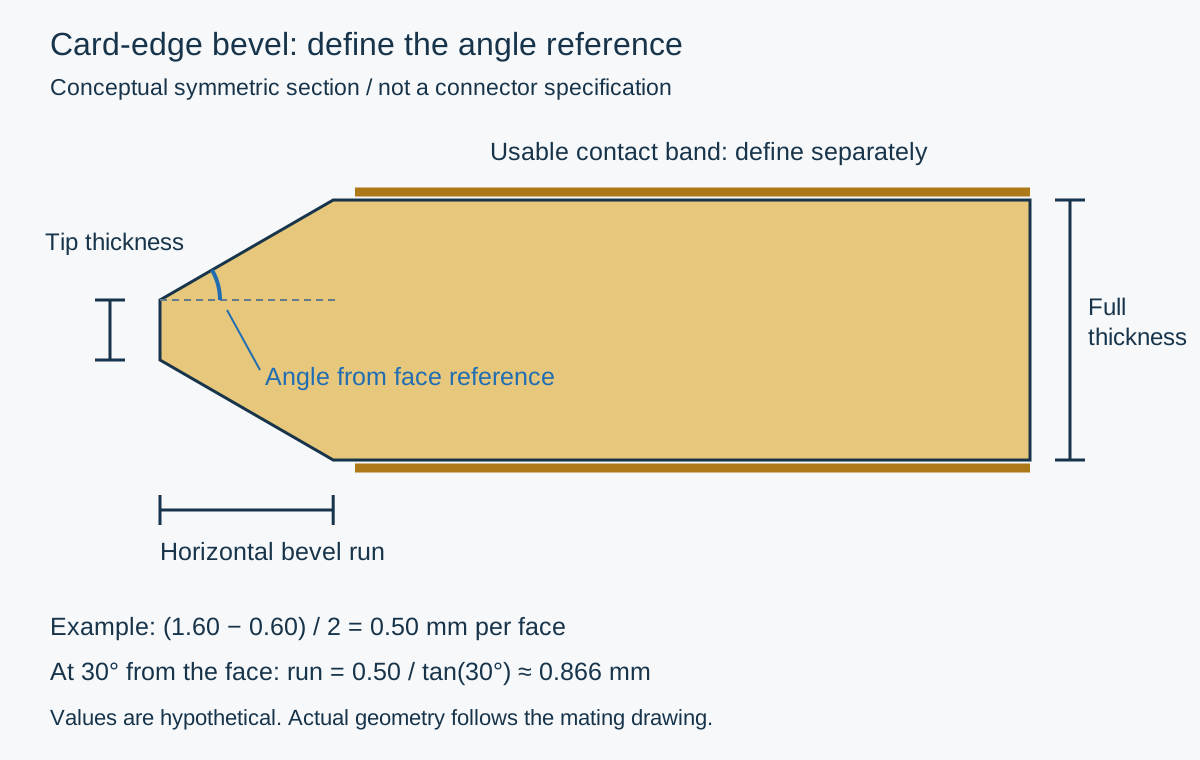
Conceptual cross-section only. The drawing defines the angle from the board face and separates the lead-in from the contact region. It is not a recommended connector geometry.
A geometric example: the angle alone does not define the edge
Assume, only for calculation, a board thickness of 1.60 mm, a symmetric two-face bevel and a remaining tip thickness of 0.60 mm. Each face loses (1.60 − 0.60) / 2 = 0.50 mm through the thickness. If the bevel angle is 30° measured from the board face, the corresponding horizontal run is 0.50 / tan(30°) ≈ 0.866 mm.
Changing the tip thickness changes that run even if the angle remains 30°. Changing the angle convention changes the calculation. These assumed values are not a socket recommendation, a process tolerance or an industry requirement. The example shows why the drawing must define more than “30° bevel.” Manufacturing variation and the socket's permitted engagement still require their own review.
Which layout details deserve a separate check?
Check mask and legend against the actual sliding-contact area. Ink, solder mask, contamination or an unintended feature in that area can interfere with the intended contact. Define the exclusions from the mating drawing and the selected fabrication process rather than applying an unexplained universal distance.
Review nearby vias and traces against the finished profile, including the bevel's material-removal envelope. A copper clearance measured from a square board outline may not describe the geometry after beveling. Inspect both sides of the card and relevant internal copper where the manufacturing operation approaches the laminate edge.
Check keying and orientation in the assembly model. A correct contact pitch does not establish correct insertion direction. If contacts have deliberately different lengths, preserve the intended sequence and verify it against the system requirements. Staggered contacts alone do not establish safe hot plugging; that depends on connector behavior, power sequencing and the complete circuit.
For high-speed interfaces, evaluate the launch and contact transition within the channel model. Hard gold and a correct bevel do not establish protocol compliance. For high-current contacts, use the connector's rating conditions and the board's electrical and thermal design rather than estimating capacity from the visible finger width alone.
How should manufacturing access and inspection be reviewed?
Ask the fabricator to review selective-plating access, temporary process connections and final profiling. The manufacturing route may need features outside the delivered outline. Agree how those features will be removed and what final edge condition is acceptable. Do not silently add permanent copper between contacts to simplify a plating operation.
Discuss panel handling and bevel-tool access alongside the assembly panelization plan. A dense panel can be economical for fabrication yet awkward for a later edge operation. Confirm which process owns the final outline and when the critical edge becomes accessible.
Inspection should separate geometry, finish and electrical connectivity. A visual check can find contamination or obvious edge damage; it does not measure gold thickness. Continuity testing can find opens or shorts; it does not demonstrate wear life. A dimensional report can establish the inspected profile, but not whether the socket contact system is qualified for the intended environment.
If a trial card is used, identify its board revision and finish and use the actual mating connector. Record observations such as seating, alignment and damage. Do not interpret one successful insertion as proof of lifetime durability. Qualification testing and acceptance criteria belong to the product's agreed validation plan.
What belongs in a gold-finger RFQ?
Submit the connector part number and controlling drawing, the board revision, fabrication data, finished card-thickness requirements and a marked mechanical section. Define the contact band on both faces, the finish for other soldering lands, contact sequencing or keying requirements and critical no-mask/no-legend areas.
Request a response to unresolved items individually: selective finish feasibility, available inspection, bevel access, process-feature removal and the evidence included in the quotation. A lower price may simply exclude a report, special operation or qualification activity. Compare the same finish area and deliverable scope before comparing totals.
Use the quote page or contact the team with the marked drawing and connector requirements. Confirm manufacturing feasibility and the available evidence for the actual build. The product design owner approves changes to contact geometry and remains responsible for the connector selection and system qualification.
Questions before release
Can ENIG be used for a prototype card?
Only if the selected connector and the intended trial permit it. Identify the deviation and expected handling. A prototype that mates successfully with ENIG does not validate a different production wear requirement.
Does thicker gold guarantee more mating cycles?
No. The complete contact system, surface condition, mating forces, environment and qualification conditions matter. Thickness is one controlled property, not an independent lifetime rating.
Are gold fingers the same as edge plating?
No. Gold fingers provide surface contacts for a mating socket. Edge plating describes metallization on a board edge and may serve another electrical or mechanical purpose. Name and draw the actual interface.
Technical reference basis
Samtec, Connector Plating FAQs, and the applicable edge-card product drawing provide the connector-side reference. Fabrication and inspection requirements must identify the agreed documents and revisions for the project. The calculation above uses declared hypothetical geometry, not a quoted manufacturing capability.