
Castellated holes are plated holes that intersect a PCB edge, leaving discrete contacts that can be soldered to matching lands on a carrier board. They let a small PCB act as a module, but the module edge and the carrier footprint must be designed and reviewed as a pair.
The critical dimensions are not just the hole diameter. The routed outline, remaining plated edge, contact pitch, module and carrier pads, finish, and assembly process all affect whether the intended connection can be made and inspected.
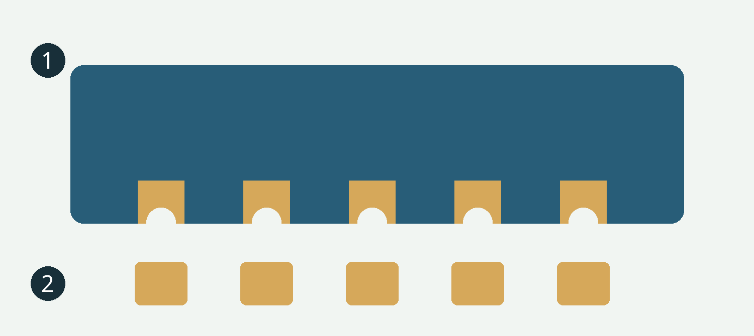
In this conceptual top view, 1 identifies module edge contacts and 2 identifies the corresponding carrier lands. The drawing is not to scale and is not a recommended footprint.
Is a castellated hole the same as edge plating?
No. A castellated contact is a discrete plated-hole feature intersecting the board outline. Edge plating instead describes metal along a specified section of the board perimeter; its purpose and geometry must be defined for that design. A row of small breakaway holes in a panel tab, often called mouse bites, serves a different purpose again: separating boards from a panel. Do not mark those three features with the same unexplained note.
APTPCB's PCB profiling page describes castellations as plated holes positioned on the routed edge. The selected stackup, geometry and manufacturing route must be compatible; availability and tolerances are confirmed for the project.
Start with the module drawing, not a generic pitch
Raspberry Pi's Pico datasheet provides one concrete example: the Pico board is 1 mm thick, has 40 through-hole positions at 2.54 mm pitch, and includes edge castellations. Its datasheet also provides a recommended carrier footprint for reflow. These numbers describe that board, not minimums or standard dimensions for all castellated PCBs.
For a purchased module, begin with its latest mechanical, footprint and assembly documentation. For a custom module, release a drawing that defines the hole locations and diameters, finished outline, contact pads, pitch, plating and finish. State the acceptable breakout of the holes at the edge and agree on tolerances with the board fabricator. The relationship between drill locations and the final outline needs review; a hole shown on an edge in a rendering is not a finished-feature specification.
On the carrier, align each land with the corresponding module contact. Check the orientation, pin numbering and any clearance around the module. If the module has an antenna or a bottom pad, follow that specific module's keepout and assembly requirements as well. An edge-contact footprint alone does not define those other interfaces.
Why should assembly review happen before fabrication?
The assembler needs more than an attractive set of lands. The carrier pad and stencil must support the intended solder deposit; module placement and board support must suit the assembly process. A module with contacts on several edges or a large bottom pad may need different paste and inspection planning from a simple two-edge part. Use the module manufacturer's recommendations and validate the proposed process for the actual board.
Panel support also matters. Tabs, rails and the separation method have to be compatible with the functional contacts and the stage at which the board is separated. Mark panel breakaway features and castellated contacts separately so the fabricator and assembler can review their interaction. Do not assume a tab can be placed over a functional contact without affecting the finished edge.
What can inspection establish?
Some edge joints are visible from the side, making their accessible surfaces easier to inspect. That view does not prove the condition of a concealed bottom pad or every part of a joint. Define the inspection method and acceptance criteria for the assembly, then agree on appropriate electrical and functional testing for the product. Appearance alone is not a substitute for those checks.
Bare-board checks and assembled-product qualification answer different questions. A fabricator can check specified board features against the released drawing and agreed acceptance requirements. The completed module and carrier still need the tests appropriate to their electrical, mechanical and operating requirements; the board drawing alone does not qualify the product.
How do the module edge and carrier land work together?
A castellated contact is part of a larger interface. On the module, the plated edge and its associated copper land need to remain connected to the intended net after the outline is formed. On the carrier, each corresponding land must align with the contact and provide the intended solderable area. The module outline, carrier footprint and pin mapping therefore need to come from the same controlled design revision.
The finished edge may not divide every plated hole into an exact half-circle. The acceptable remaining contact geometry is a drawing and fabrication question, not something that can be established from a generic illustration. Define the intended outline, hole center and finished-feature condition, then ask the fabricator how the design will be produced and checked. State the applicable plating and finish requirements without assuming that an ordinary board-edge note also defines every contact.
The carrier layout should also account for the module body's position and any parts that protrude underneath. A footprint that aligns in two dimensions may still conflict with a nearby component, enclosure wall or connector when assembled. For a radio module, use its own antenna and ground instructions and evaluate the surrounding carrier and enclosure; changing a mechanical clearance can affect the final product even when the edge contacts themselves fit.
Compare the interface with other connection choices
| Connection approach | Useful when | Question before choosing |
|---|---|---|
| Castellated module | A soldered module-to-carrier connection fits the product and assembly plan. | Can both boards be built, aligned, inspected and reworked as the product requires? |
| Pin headers or sockets | The design needs a connector interface or removable module. | Do height, contact count, retention and component sourcing meet the product requirements? |
| Other board-to-board contacts | The mechanical package or contact requirements favor a different interface. | Are the mating parts, tolerances, assembly steps and validation conditions defined together? |
No option is automatically smaller, stronger or cheaper for every product. Connector cost is only one part of the comparison: include board fabrication, placement, inspection, service access, rework and the required reliability testing. A soldered module may make field replacement less convenient; a removable connector adds a separate mating interface that must be selected and qualified.
A sample design review for a custom module
Suppose a designer places edge contacts on two sides of a small controller module. The carrier team needs the connector map and orientation before building the footprint. The board fabricator needs the final outline, hole table, copper pads, finish, thickness and a clear statement that the marked holes are functional castellations. The assembly team needs the module and carrier layouts, component heights, proposed stencil and intended reflow constraints.
During review, the team notices that a proposed panel tab would cross one of the contact areas. That is not just a panel drawing detail: it may change the finished contact edge or the order in which the board can be separated. The teams can move the tab, revise the panel, or discuss another feasible production route. The selected option and edge acceptance criteria belong in the approved manufacturing package.
This is a hypothetical design review, not an APTPCB customer case or evidence of a specific production method. Its purpose is to show why the module, carrier and panel should be checked together before ordering tooling or assembling a batch.
Investigating an assembly problem
| What is observed | Investigate first | Evidence that helps |
|---|---|---|
| Contacts do not line up with carrier lands | Module orientation, pin numbering, released footprints and actual board outlines. | Module and carrier revisions, placement data and dimensional inspection. |
| A visible joint looks poorly wetted | Finished surfaces, storage and handling, paste deposit and the qualified assembly process. | Module documentation, process records and inspection images; avoid assuming one cause from appearance. |
| Adjacent contacts appear bridged | Carrier land and mask geometry, paste deposit, placement and assembly conditions. | Footprint, stencil revision, board images and continuity or isolation checks. |
| The module does not sit as intended | Board flatness, bottom components or pads, deposit and mechanical interference. | Assembly drawing, height constraints and observed placement; inspect hidden interfaces using an agreed method. |
| The assembly passes visual inspection but fails operation | Power, programming, interfaces and accessible and hidden connections. | Electrical test results, firmware and configuration, inspection findings and the product test plan. |
Record the module and carrier revisions and preserve the as-found condition before repair. Visual inspection, electrical checks and functional testing cover different questions; the appropriate method and acceptance criteria depend on the design. If destructive analysis is required, agree on the sampling and failure-analysis plan before cutting or reworking a unit.
What belongs in a complete RFQ?
For fabrication, provide the design files and a dimensioned drawing that distinguishes plated castellations, any continuous plated-edge sections and panel breakaway features. Identify board thickness, stackup, finish, contact locations and the required edge condition. Clarify whether the boards are supplied individually or in a panel and when separation occurs.
For assembly, add the module and carrier revisions, BOM, placement information, assembly drawing, applicable module documentation and any inspection or test requirements. Identify who supplies the module, whether a stencil is already available, and who approves changes to the footprint or assembly process. Request written clarification where a proposed process, tolerance or inspection report is essential to the decision. The PCB assembly cost comparison explains why scope must be aligned before comparing prices.
Handoff the complete interface
| Interface | Provide for review | Decision to resolve |
|---|---|---|
| Module PCB | Outline, hole and pad geometry, thickness, finish, plating and acceptable breakout | Can the specified edge be fabricated and inspected with the proposed stackup and panel? |
| Carrier PCB | Matching footprint, orientation, land geometry and applicable keepouts | Does each contact align, and is there space for the module and its other interfaces? |
| Assembly | Module documentation, placement, stencil and panel requirements | Are paste, support and the intended assembly sequence appropriate for this combination? |
| Verification | Drawing tolerances, inspection and test requirements | What is checked on the bare board and assembly, and what remains a product-level qualification? |
The Gerber file article and layout DFM guidelines explain the wider file handoff. Send the module and carrier information with a quote request, or contact APTPCB to discuss edge geometry and project-specific tolerances.