
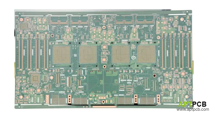
KB-6167GLD is Kingboard's laminate designation for a halogen-free, high-Tg, low-loss FR-4 system; KB-6067GLD is its companion prepreg. It is intended for applications such as servers, switches, and base-station hardware, but the material name alone does not prove that a PCB will meet a 25G, 56G, PCIe, RF, or other channel target.
Key Takeaways
- Kingboard positions KB-6167GLD as halogen-, antimony-, and red-phosphorus-free, with low Dk/Df, low Z-axis expansion, thermal reliability, and anti-CAF capability.
- Published values are typical reference values. Release a design against the current official technical information, its test methods and conditions, and the exact laminate/prepreg construction.
- Channel performance depends on dielectric construction, copper profile, trace geometry, vias, launches, connectors, route length, and the complete loss budget—not a laminate label or fixed data-rate claim.
- A material substitution requires impedance recalculation and may require new loss, thermal, CAF, assembly, and reliability evidence.
- Put stack-up inputs, approved alternatives, coupons, test limits, documents, and change-control rules into the RFQ before material is purchased.
Table of Contents
- What is KB-6167GLD?
- What does the official material positioning prove?
- How should Dk and Df be qualified?
- Can KB-6167GLD support 25G or 56G channels?
- How should the stack-up and copper be specified?
- Can another laminate replace KB-6167GLD?
- What fabrication controls matter?
- Which coupons and tests should be requested?
- Common failure modes
- Cost and lead-time drivers
- RFQ checklist
- Standards and responsibility boundary
- FAQ
What is KB-6167GLD?
KB-6167GLD is the rigid copper-clad laminate in the material system, while KB-6067GLD is the prepreg used to bond multilayer constructions. Kingboard describes the system as halogen-free, high-Tg, and low-loss, with low Dk/Df, very low Z-axis CTE, anti-CAF capability, and thermal reliability.
Those descriptors make the material a candidate for high-layer-count and signal-integrity-sensitive hardware. They do not replace a released stack-up or product qualification.
| Material-system element | What must be defined for a real build |
|---|---|
| KB-6167GLD laminate | Core construction, thickness, copper foil, lot, technical-information revision, and permitted tolerances |
| KB-6067GLD prepreg | Glass style, resin content, target pressed thickness, flow requirements, and storage controls |
| Transmission lines | Layer, geometry, reference planes, mask state, target impedance, tolerance, and allowed production adjustment |
| Loss-sensitive paths | Frequency range, length, via and launch structures, connector model, copper requirement, and channel limit |
| Reliability | Assembly profile, environment, via geometry, CAF or thermal-cycle plan, and acceptance evidence |
| Change control | Approved equivalents, notification trigger, re-analysis, requalification, and customer approval authority |
For a broader view of the manufacturer's portfolio, see the Kingboard laminate selection guide. KB-6167GLD should still be qualified as a specific system rather than as generic “high-Tg FR-4.”
What does the official material positioning prove?
The current supplier document is the starting authority. It identifies the product family, intended characteristics, test methods, specimen conditions, application guidance, and typical values. Because those values are stated as reference data, they should not silently become guaranteed finished-board limits.
| Supplier statement | Useful engineering interpretation | What it does not prove |
|---|---|---|
| Low Dk/Df | Candidate for lower dielectric loss and controlled transmission-line design | Finished-channel loss, reach, eye margin, or protocol compliance |
| High Tg and thermal reliability | Input to fabrication and assembly thermal review | Continuous operating temperature, unlimited reflow, or plated-via life |
| Extremely low Z-axis CTE | Favorable input for through-thickness expansion risk | Reliability of every hole geometry, plating process, or assembly profile |
| Anti-CAF capability | Material system is designed to resist conductive anodic filament growth | Product CAF life without spacing, humidity, bias, process, and test definition |
| Halogen-, antimony-, and red-phosphorus-free | Supports a halogen-free material strategy | Finished-product environmental compliance without current declarations and exact construction coverage |
| Server, switch, and base-station applications | Indicates intended market positioning | Automatic suitability for a specific platform or interface |
Before release, obtain the current KB-6167GLD/KB-6067GLD technical information and any required processing guide, declaration, recognition record, or certificate. Record the revision in the purchase specification so a later document or formulation change is visible.
How should Dk and Df be qualified?
Dk and Df are not context-free constants. Their reported values depend on test method, frequency, specimen construction, resin content, glass style, conditioning, and whether the number is a nominal, typical, specification, or design value. A field solver also needs the geometry and copper assumptions used by the production stack-up.
Use this datasheet-to-stack-up matrix before approving the material:
| Property or input | Official evidence to capture | Design-model input | Fabrication control | Release evidence | Owner |
|---|---|---|---|---|---|
| Dk | Method, frequency, specimen, construction, and revision | Construction-appropriate Dk or correlated design value | Core/prepreg style, RC, and pressed thickness | Approved stack-up and impedance correlation | SI/design + fabricator |
| Df | Method, frequency, conditioning, and revision | Dielectric-loss input across the required band | Material identity and construction | Representative loss coupon when required | SI/test + fabricator |
| Copper | Foil type and available profile data | Roughness model and finished copper | Approved foil, treatment side, plating, and etch | Material record and dimensional evidence | Design + sourcing + fabricator |
| Dielectric geometry | Core and prepreg options | Finished dielectric thickness | Layup, resin demand, press cycle, and thickness tolerance | Cross-section or thickness report | Fabricator |
| Z-axis behavior | Method and condition | Via and thermal-reliability assumptions | Cure, board thickness, drill, desmear, and plating | Microsection and project qualification | Reliability + fabricator |
| CAF behavior | Test method and specimen conditions | Spacing and environmental risk assumptions | Cleanliness, hole-wall quality, moisture, and process control | Project-specific CAF evidence if required | Reliability/quality |
Do not copy a single catalog Dk into every impedance or loss model. Prepreg resin content and pressed thickness can change the effective dielectric behavior even within the same product family. The PCB stack-up design guide explains how material inputs, geometry, and production tolerances should be released together.
Can KB-6167GLD support 25G or 56G channels?
It may be a candidate, but there is no universal yes/no answer based only on the material designation. A serial data rate does not specify route length, transmitter and receiver capability, equalization, connector loss, via topology, insertion-loss limit, return-loss limit, crosstalk, or manufacturing variation.
Evaluate the full channel:
- Define the protocol, data rate, Nyquist frequency, compliance point, and required margin.
- Model dielectric and conductor loss using the proposed construction and copper treatment.
- Include trace length, neck-downs, vias, unused stubs, connector launches, connectors, packages, and any cables.
- Review impedance discontinuities, return paths, crosstalk, skew, glass-weave sensitivity, and reference-plane transitions.
- Correlate the model with a representative coupon or test vehicle when the risk justifies it.
- Validate the assembled channel under the protocol's required method; a bare-board coupon does not certify the final system.
| Question | Evidence needed before saying “supported” |
|---|---|
| Does the trace meet the loss budget? | Stack-specific model plus defined coupon or test-vehicle correlation |
| Is a plated-through via acceptable? | Via model including barrel, pads, antipads, return vias, and unused stub |
| Is backdrilling required? | Modeled or measured stub response and a drawing-defined residual-stub limit |
| Does PAM4 performance pass? | Complete channel analysis and protocol/system validation, not Df alone |
| Can the route length increase? | Updated channel budget with manufacturing and environmental margin |
| Is the build production-ready? | Frozen material, stack-up, foil, process, coupons, limits, and change control |
For the wider material-and-geometry workflow, use the high-frequency PCB fabrication guide. It separates material properties from the complete transmission path.
How should the stack-up and copper be specified?
The released stack-up should name KB-6167GLD cores and KB-6067GLD prepregs precisely enough to prevent an unreviewed change in resin content, glass construction, pressed thickness, copper profile, or impedance geometry.
Stack-up controls
- Exact core and prepreg designation, construction, resin content, and target finished dielectric thickness
- Finished board thickness, copper weights, plating assumptions, layer symmetry, and copper distribution
- Controlled-impedance geometry, reference plane, tolerance, solder-mask state, and coupon structure
- Resin-fill needs around dense copper, buried features, via fill, or local copper imbalance
- Sequential lamination, blind/buried vias, via-in-pad, controlled-depth drilling, and registration requirements
Copper controls
Copper surface treatment affects conductor loss, especially as frequency rises and the current is concentrated near the conductor surface. “Use VLP” is still incomplete: foil availability, treatment side, profile terminology, roughness metric, model, peel strength, and compatibility with the chosen construction must be agreed.
Specify an exact approved foil or a measurable, supplier-supported requirement when conductor loss is material to the budget. Do not publish a universal roughness value or loss-reduction percentage unless it comes from the selected foil data and the same modeling or test conditions.
Can another laminate replace KB-6167GLD?
Do not treat a similar Dk/Df, Tg, IPC slash sheet, or marketing category as proof of interchangeability. A substitution can alter line width, dielectric thickness, resin flow, dimensional movement, lamination, drilling, loss, CAF behavior, documentation, and qualification status.
Use this change-control checklist:
| Comparison item | Minimum review |
|---|---|
| Dk and Df | Compare values, methods, frequency, conditioning, specimen, and whether each value is typical or guaranteed |
| Laminate/prepreg set | Compare resin chemistry, glass styles, resin-content options, flow, and pressed-thickness availability |
| Copper foil | Compare foil type, treatment, roughness data, bond performance, and availability |
| Stack-up | Recalculate finished geometry, impedance, loss, total thickness, symmetry, and resin demand |
| Fabrication | Review storage, conditioning, dimensional compensation, lamination, drilling, desmear, and plating compatibility |
| Reliability | Reassess Z-axis behavior, thermal excursions, via structures, moisture, CAF, and product environment |
| Test correlation | Decide whether impedance, insertion loss, thermal, CAF, or system tests must be repeated |
| Compliance and sourcing | Verify current declarations, recognition scope, approved-source status, lot traceability, and continuity plan |
| Approval | Define who may authorize the change and which documents must be revised |
Compare KB-6167GLD with KB-6167F, KB-6167GMD, or KB-3200G only against the actual project requirements and current supplier documents. These names describe different material choices; they are not automatic drop-in equivalents.
What fabrication controls matter?
A low-loss laminate does not protect the design from ordinary fabrication variation. The build still depends on disciplined material handling, lamination, imaging, etching, drilling, hole-wall preparation, plating, and inspection.
| Process stage | Control question | Useful evidence |
|---|---|---|
| Incoming material | Is the laminate/prepreg, lot, foil, thickness, document revision, and storage history correct? | Receiving record, labels, certificate/declaration, and lot traceability |
| Inner-layer imaging | Will finished line width and spacing match the impedance model? | CAM notes, etch compensation, measured features, and coupon correlation |
| Lamination | Will resin fill, pressed thickness, registration, cure, and symmetry meet the released stack-up? | Layup traveler, material-temperature/pressure record, thickness and registration data |
| Drilling | Are tool, feed, speed, stack height, hit count, entry/backup, and dust control suitable? | Drill records and representative hole-wall microsections |
| Desmear and plating | Is smear removed without damaging glass/resin, and is copper continuous at interfaces? | Chemistry controls, microsection, and plating-thickness evidence |
| Backdrilling | Is it electrically required and mechanically achievable without threatening adjacent layers? | Drawing-defined side, target layer, diameter, keep-out, and residual-stub evidence |
| Final inspection | Do dimensions, holes, copper, impedance, continuity, and requested coupons meet the purchase criteria? | Inspection, electrical-test, microsection, TDR, or VNA report as specified |
Backdrilling is not mandatory for every KB-6167GLD board. Specify it only after the via transition has been evaluated, and define the permitted residual stub from that evaluation rather than using a universal number.
Which coupons and tests should be requested?
Test language must identify the structure, method, frequency or time domain, fixtures, calibration, limits, sampling, and report format. “Test to 20 GHz” or “perform SI testing” is not an acceptance specification.
| Evidence | What it answers | Required definition |
|---|---|---|
| Material and lot record | Was the approved laminate, prepreg, and foil used? | Exact documents, revision, lot linkage, and retention |
| Microsection | Do sampled dielectric, registration, hole wall, plating, interfaces, and backdrill meet criteria? | Feature, location, sampling, measurement, and limits |
| TDR coupon | Does the defined transmission line meet the impedance target and show major discontinuities? | Coupon geometry, reference, target, tolerance, method, and reporting |
| VNA loss structure | What are reflection and transmission versus frequency for the tested structure? | Ports, frequency range, fixture, calibration/de-embedding, limits, and Touchstone/report format |
| CAF or thermal test | Does the defined test vehicle survive the specified environment? | Vehicle, conditioning, bias/profile, duration, sample size, failure criteria, and disposition |
| System compliance test | Does the assembled product meet the interface requirement? | Protocol method, compliance point, fixtures, software, environmental condition, and margin rule |
A coupon should represent the product geometry and material construction closely enough to answer the stated question. A passing impedance coupon does not prove insertion loss, and a passing bare-board loss coupon does not prove the connector, package, or assembled channel.
Common KB-6167GLD PCB failure modes
| Symptom | Likely control gap | Corrective evidence |
|---|---|---|
| Impedance differs from the model | Wrong Dk basis, prepreg RC/thickness change, copper/profile mismatch, etch or mask variation | Approved stack-up, measured geometry, TDR coupon, and material record |
| Insertion loss exceeds budget | Df method mismatch, rough copper, narrow/long route, vias, launches, connectors, or fixture error | Updated channel model, foil data, calibrated VNA result, and structure correlation |
| Resonance near a via | Unused stub, pad/antipad geometry, weak return path, or launch discontinuity | Via model, residual-stub plan, return-via review, and representative measurement |
| Board thickness or resin fill misses target | Prepreg substitution, incomplete resin-demand analysis, copper imbalance, or press variation | Layup record, RC, press data, thickness map, and cross-section |
| Registration or warpage varies | Uncontrolled scale compensation, asymmetric construction, press/cool variation, or panel handling | Layer-scale data, symmetry review, press record, and dimensional map |
| Hole reliability is weak | Drill damage, smear, plating/interface defect, via geometry, or excessive thermal exposure | Microsection, plating data, assembly profile, and project reliability test |
| Repeat build behaves differently | Material, foil, stack-up, process, test method, or supplier document changed | Frozen baseline, lot traceability, deviation record, and requalification decision |
What drives KB-6167GLD PCB cost and lead time?
The material name is only one cost input. Quote variance usually comes from stock status, minimum material purchase, foil and construction availability, stack-up complexity, controlled features, test evidence, and qualification scope.
- Exact KB-6167GLD/KB-6067GLD construction, panel size, stock, lot restrictions, and approved alternatives
- Copper foil type, profile requirement, thickness, and sourcing lead time
- Layer count, board thickness, fine geometry, sequential lamination, HDI, filled via-in-pad, and registration controls
- Backdrilling, controlled-depth features, tight mechanical tolerances, and representative coupons
- TDR, VNA, microsections, environmental tests, documentation, sampling, and retained records
- Prototype correlation, qualification build, repeat-order controls, and customer approval for changes
A hybrid stack-up may reduce premium-material usage, but it can also add compatibility, lamination, modeling, sourcing, and qualification work. Compare the total validated build—not a material price index—before choosing it.
KB-6167GLD PCB RFQ checklist
Design package
- Gerber, ODB++, or IPC-2581 data; drill files; netlist; fabrication drawing; revision readme; and controlled panel data if applicable
- Layer count, finished thickness, copper, surface finish, mask, mechanical tolerances, controlled depths, via structures, and aspect-ratio constraints
- Proposed stack-up naming KB-6167GLD cores, KB-6067GLD prepregs, constructions, resin contents, finished dielectric thicknesses, and copper foil
Electrical requirements
- Protocol or operating band, critical nets, route lengths, transmission-line type, reference planes, impedance, tolerance, and mask state
- Loss, return-loss, crosstalk, skew, or delay limits only where required and testable
- Launch, connector, via, pad, antipad, return-via, backdrill, and glass-weave controls used by the released model
- Coupon or test-vehicle geometry, TDR/VNA method, fixtures, calibration/de-embedding, sampling, limits, and report format
Reliability and documentation
- Assembly alloy/profile, number of thermal excursions, rework limits, operating/storage environment, and intended qualification tests
- Material revision, lot traceability, required declarations or recognition evidence, microsection, dimensional report, and electrical-test records
- Approved substitutions, notification timing, approval authority, re-analysis and requalification triggers, and deviation handling
- Prototype and production quantities, forecast, destination, assembly scope, target schedule, and record-retention needs
Standards and responsibility boundary
References that may apply include:
- IPC-4101 — Specification for Base Materials for Rigid and Multilayer Printed Boards
- IPC-6012 — Qualification and Performance Specification for Rigid Printed Boards
- IPC-2221 — Generic Standard on Printed Board Design
- IPC-2141 — Design Guide for High-Speed Controlled Impedance Circuit Boards
- IPC-TM-650 — Test Methods Manual
- IEC 61249-2-21 — Halogen-Free Base Materials for Printed Boards
- UL 94 — Tests for Flammability of Plastic Materials
- Kingboard KB-6167GLD / KB-6067GLD Technical Information
Confirm the current revision, applicable slash sheet, contract hierarchy, test method, construction, and acceptance criteria for the project. Any UL, environmental, halogen-free, flammability, CAF, or other statement should be verified against current supplier records and the exact material construction being purchased.
KB-6167GLD can support a material strategy, but it does not certify the finished PCB or product. Final signal integrity, EMC, safety, reliability, regulatory compliance, and protocol performance remain product-level responsibilities.
KB-6167GLD PCB FAQ
What is KB-6167GLD?
KB-6167GLD is Kingboard's halogen-free, high-Tg, low-loss FR-4 laminate designation for multilayer PCB applications. KB-6067GLD is the companion prepreg.
Is KB-6167GLD a low-loss material?
Kingboard positions it as low-loss and lists low Dk/Df among its characteristics. Use the current official values, test conditions, exact construction, copper profile, and complete channel model before approving it for a loss-sensitive path.
What is the Dk or Df of KB-6167GLD?
Use the current official technical information rather than an uncited web value. Dk and Df must be interpreted with their frequency, method, specimen, resin content, conditioning, and typical-versus-guaranteed status.
Can KB-6167GLD support 25G Ethernet or 56G PAM4?
Possibly, but the material name alone cannot prove compliance. Suitability depends on the protocol budget, route length, geometry, copper, vias, launches, connectors, packages, equalization, manufacturing variation, and system validation.
Is KB-6167GLD equivalent to Panasonic Megtron 4?
Do not treat them as interchangeable without a documented comparison. Review Dk/Df methods, constructions, prepregs, copper, thermal and CAF behavior, processing, availability, compliance records, stack-up changes, and requalification needs.
Does every KB-6167GLD PCB need VLP copper?
No. Lower-profile copper may help when conductor loss materially affects the channel budget, but the requirement should come from the model, available foil data, construction, bond needs, and validation plan.
Does every KB-6167GLD PCB need backdrilling?
No. Backdrilling is appropriate when the modeled or measured unused via stub creates unacceptable reflection or loss. Specify the side, target layer, drill diameter, keep-outs, and residual-stub limit when it is required.
Which tests should be specified for a KB-6167GLD PCB?
Specify only tests tied to acceptance needs: material records, electrical test, dimensions, microsections, TDR impedance, VNA S-parameters, CAF, thermal testing, or a system compliance test. Each requires a defined structure, method, limits, sampling, and report format.
Can KB-6167GLD be used in a hybrid stack-up?
Potentially. Review resin and process compatibility, Dk/Df, pressed geometry, copper, symmetry, lamination, registration, reliability, and the qualification burden before assuming that a hybrid build reduces total cost.
What should be included in a KB-6167GLD PCB quote request?
Provide fabrication data, the exact material and stack-up, copper foil, impedance and loss requirements, via and backdrill details, assembly profile, environment, coupons and tests, documentation, quantities, schedule, approved substitutions, and change-control rules.
Request a KB-6167GLD PCB review
Send the stack-up, material revision, copper requirement, critical channels, via and launch details, loss budget, coupons, test limits, qualification needs, quantities, and substitution rules. APTPCB will review the submitted requirements for manufacturability and quotation; final materials, capabilities, and acceptance evidence are confirmed against the released project specification.