
A PCB thermal relief is a pad-to-copper connection that uses narrow copper spokes instead of joining the pad to the surrounding plane along its entire perimeter. The spokes maintain an electrical connection while restricting some heat flow away from the pad during soldering. This can make it easier to bring a connection attached to a large copper area to soldering temperature.
The tradeoff matters: the same restriction that helps during assembly also affects the electrical and thermal path during operation. A low-current connector pin, a high-current terminal and the exposed heat-transfer pad under a power device do not necessarily need the same connection. Choose the geometry for the actual circuit and assembly process, then verify it with the fabricator and assembler.
For the complete soldering operation, see through-hole soldering basics. For temperature control during surface-mount assembly, see reflow profile basics. The decision here is the copper connection at the pad or via and how it interacts with those processes.
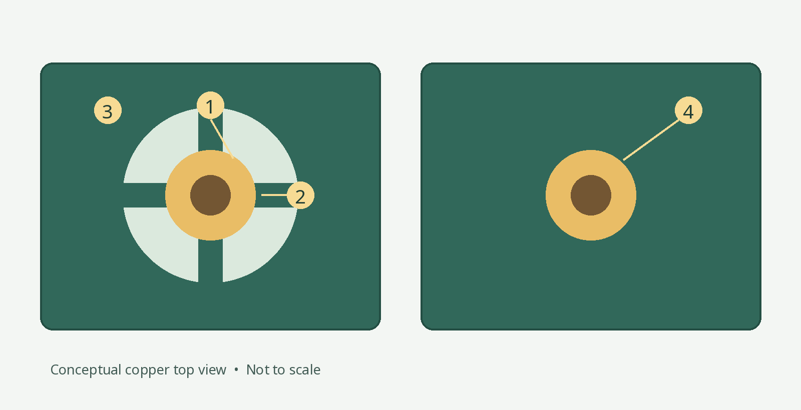
The drawing is a conceptual top view, not a manufacturing pattern or a dimensional recommendation. 1 is the pad, 2 the copper spokes, 3 the surrounding copper and 4 a direct copper connection. The visible gap is a copper clearance; it is not automatically a solder-mask opening. The number and dimensions of spokes must be chosen for the design.

Real circuit-board photograph showing soldered joints and traces; the image does not identify the underlying pad-to-plane connection. Photo: Tima Miroshnichenko / Pexels.
Why can a large copper plane make a joint harder to solder?
A solder joint must reach a suitable temperature for the solder and flux being used. When a pad is connected to a substantial copper area, some of the supplied heat flows into that copper as the joint warms. The amount depends on the copper geometry and thickness, the connections on other layers, the component, board and soldering process.
For a through-hole connector attached to a ground plane, the assembler may need to heat not only the lead and visible pad but also the plated barrel and connected copper. If the joint does not receive the required heat under the qualified process, wetting or hole fill may be inadequate. A spoke connection can reduce one path by which heat leaves the pad, making the joint easier to heat. It is not a substitute for a suitable flux, clean surfaces, joint design or a controlled soldering process.
The effect is different for a surface-mount component passing through a reflow oven. If the two ends of a small part have substantially different copper connections, they may heat differently. That is one factor to examine when a part lifts or shifts during reflow; paste deposits, placement, component geometry and the actual temperature profile also matter. Do not diagnose tombstoning from copper shape alone.
Thermal relief, thermal pad and thermal via: different jobs
These terms sound similar but describe different features:
- A thermal relief connection is the spoke-like copper connection between a pad or via and a surrounding plane or pour.
- An exposed thermal pad is a package feature, often on the underside of an IC, intended to connect to a corresponding board land for heat transfer and sometimes an electrical connection.
- A thermal via is a via used as part of a path that carries heat between board layers or surfaces.
- A solder-mask opening exposes an area of copper for soldering or another purpose; it is defined separately from the copper relief geometry.
A thermal relief can slow heat leaving a solder joint during assembly. An exposed thermal pad and its thermal vias may be designed to carry heat away from an operating device. Applying spoke connections to every pad and via because the CAD default says “thermal” can therefore undermine the intended heat path.
Texas Instruments' Best Practices for Board Layout of Motor Drivers, SLVA959B, illustrates this distinction for its motor-driver context: a solid connection at the relevant thermal vias provides a less constricted heat path to the copper layers. Its PowerPAD Layout Guidelines, SLOA120, makes a similar recommendation for the construction discussed there. These are examples of component and application guidance, not proof that every power pad or every via must use the same connection. Follow the specific component documentation and evaluate the complete board.
Relief or direct connection: which question comes first?
| Connection being reviewed | Why a relief may be considered | Why a direct connection may be considered | Evidence to agree |
|---|---|---|---|
| A soldered through-hole pin tied to a large plane | Reduce heat flow into the plane while the joint is heated. | Preserve a stronger copper path where electrical or thermal demands require it. | Joint design, solder process, inspection method and electrical requirements. |
| A small two-terminal surface-mount part | Help review thermal balance between its two pads. | Retain the needed electrical path or a component-specific land pattern. | Paste and pad geometry, copper on each side, placement and reflow behavior. |
| A power terminal or current-carrying pad | Make soldering feasible if the geometry is adequate for the load. | Provide more copper connection area where required by current and temperature-rise analysis. | Load profile, copper geometry, temperature limits and assembly validation. |
| An exposed power-device pad or heat-transfer via | A relief could be relevant to a separate soldering need only if it does not defeat the intended design. | Preserve the heat path specified for the component and board. | Component land pattern, thermal path, via treatment and measured or analyzed device temperatures. |
| An RF ground or signal-related connection | Assembly still needs a repeatable process. | Preserve a reference or grounding geometry selected for electrical performance. | Component layout guidance and RF or signal-integrity analysis for the actual structure. |
A table cannot decide these connections by itself. The designer owns the circuit and performance requirements; the fabricator and assembler can review whether the proposed copper geometry can be made and soldered with the agreed process. When the preferred electrical or heat path makes soldering difficult, discuss the process and layout together rather than silently narrowing the connection.
What do spoke width, count and gap change?
A relief contains copper spokes, a pad and a gap between the pad and the surrounding pour. For otherwise comparable geometry, wider or more effective spokes generally reduce electrical resistance and conduct more heat into the plane, which can also increase the heat needed to bring the joint to soldering temperature. A larger gap generally lengthens the spokes and restricts those paths more, but can also affect copper around neighboring features. These interacting variables describe directional effects, not a current rating; assess them together in the actual generated geometry.
Consider the geometry that will actually be fabricated. A CAD rule may request several spokes, but nearby clearances, an adjacent pad, the board outline or a competing copper region can alter what the fill produces. A thin spoke may also be constrained by the fabricator's minimum feature and registration capabilities. Check the resulting copper on every relevant layer after refilling zones and generating manufacturing outputs. The specified settings and the finished copper pattern are not necessarily identical.
There is no universal spoke count, width, gap or current limit suitable for every board. Do not multiply a generic trace-current value by the number of visible spokes and call the pad approved. Current distribution, copper thickness, geometry, temperature, nearby heat sources, tolerances and the rest of the circuit matter. For a demanding connection, the design authority should use an appropriate analysis and validation plan for the actual structure.
A worked geometry check
Suppose a round pad is 1.20 mm in diameter and the layout calls for a 0.22 mm radial relief gap on each side. In this hypothetical, concentric example, the nominal outer boundary of the cleared region is:
1.20 mm + 2 × 0.22 mm = 1.64 mm
The value describes the maximum outside diameter of the clearance region before considering adjacent features; the copper spokes still cross the gap. It is not the drilled-hole diameter, the solder-mask opening, a recommended gap or a finished-board tolerance. For an oblong or custom-shaped pad, inspect the actual generated geometry rather than treating it as a circle. Confirm the fabricator's minimum copper and clearance rules for the chosen stackup and copper weight before approving any dimensions.
This drawing check is not an APTPCB manufacturing specification or a current or heating calculation: spoke width, actual connected spoke count, inner-layer copper and soldering process remain separate inputs.
Check the actual CAD output
In a zone-based CAD tool, check the connection setting for the relevant zone, footprint and individual pad, then refill the copper and inspect the resulting shape on each affected layer. Look for a missing spoke, an isolated copper island or a solid connection left on an internal layer. Run connectivity and design-rule checks, then inspect the exported copper layers with the drill and mask outputs.
For example, KiCad's PCB Editor 10.0 documentation describes pad and footprint connection overrides as well as zone settings for relief gap and spoke width. It also records a version-sensitive detail: before KiCad 9, entering 0 for a pad's relief gap or spoke width caused inheritance; in KiCad 9 and later, 0 is an explicit value, while a blank field inherits. Confirm the version and actual generated fill before changing an existing design. Other CAD tools have their own rules and may use different terminology.
Through-hole pins and surface-mount pads need separate checks
For a plated through-hole, look beyond the top-layer annular ring. The barrel may connect to copper on several layers, each with its own pad and plane relationship. The proposed relief pattern should be reviewed in the context of the drill, finished hole, internal connections, component lead and soldering method. A good-looking top surface alone does not show the full condition of the joint; inspection and acceptance should follow the requirements agreed for the product.
For a surface-mount pad, compare the complete copper environment of all relevant terminals. One pad may connect directly to a large pour while the other connects to a narrow trace. Another layer or nearby via can also carry heat away. If the assembly team sees inconsistent reflow or a lifted part, review the paste deposits, part orientation, placement, profile and copper connections together before changing only the relief setting.
A solder mask does not determine whether the pad is connected by spokes or solid copper. Copper and mask are separate fabrication layers. A mask-defined land, a copper-defined land and a relief connection answer different geometric questions. Review both copper and mask outputs against the component's land-pattern guidance and the fabricator's rules; see solder mask clearance and dam rules for the mask-specific discussion.
A hypothetical board with three different connections
Imagine a controller board with a low-current through-hole signal connector, a supply connector carrying substantial current and a motor-driver IC with an exposed pad intended to move heat into the board. All three touch large copper areas, but a single global “thermal relief everywhere” setting would leave three different questions unanswered.
| Connection | Conditional candidate | What to verify before release |
|---|---|---|
| Low-current signal connector | Start with thermal relief if there is no special electrical constraint and the generated spokes satisfy the design and fabrication rules. | The actual copper on all connected layers, electrical adequacy, and heating and inspection with the planned soldering method. |
| Supply connector | Start with a solid connection if analysis shows that the proposed spokes exceed the allowed voltage drop or temperature rise. | The complete current path under the specified load; adjust the soldering process for the greater thermal load and verify joint quality. |
| Motor-driver thermal vias | Use the solid structure required by the exact component documentation where that guidance calls for a complete heat-transfer connection. | The specified exposed-pad and via construction, electrically correct plane connections, assembly requirements and operating device temperature. |
These are candidate decisions for this hypothetical board, not test results, an APTPCB customer case or general current thresholds. Record the affected pads and layers, the reason for each exception and the evidence needed for release. A global rule can therefore have documented local exceptions.
What should you check when soldering is difficult?
| Observation | Check before changing the layout | Possible follow-up |
|---|---|---|
| A through-hole joint is slow to heat. | Connected copper on all layers, lead and hole geometry, preheat, flux and soldering method. | Review a relief connection or an assembly-process change against the electrical requirement. |
| One end of a small component lifts or shifts. | Paste amount, placement, pad geometry, copper imbalance and the measured profile. | Adjust the verified cause; compare both pad connections after any change. |
| A current-carrying pad runs hotter than expected. | Load and duty cycle, actual copper and spoke geometry, joint condition, measurement position and other heat sources. | Reassess the electrical path and temperature under the specified operating conditions. |
| A power IC is hotter than expected. | Part mounting, exposed-pad soldering, copper and thermal-via connections, board-to-enclosure path and operating conditions. | Compare with the component manufacturer's thermal guidance and validate the revised board. |
| A CAD pad appears disconnected after a pour. | Net assignment, zone priority, clearances, minimum spoke geometry and pad-specific overrides. | Correct the approved design, refill zones, rerun connectivity checks and inspect the plotted layers. |
These are starting points for investigation. Do not increase iron temperature, change a reflow recipe or widen a copper connection without checking component limits, the assembly process and the effect on the rest of the board.
Compare two candidate connections before release
If the soldering and operating requirements pull in different directions, use representative samples to compare proposed geometries rather than choosing from a generic current threshold. For example, a team might build candidate A with an agreed spoke connection and candidate B with a direct connection for the same through-hole pin. This is a proposed experiment, not a measured result:
- Record the board revision, copper layers and finished construction, pad and hole dimensions, and the actual generated connection on every affected layer for each candidate.
- Keep the component, solder alloy, flux, board handling and intended assembly process consistent; record any process differences and the sample size. Include the real production soldering method, rather than assuming hand soldering represents a wave or selective process.
- Define the project acceptance criteria before testing. Inspect the joints using the agreed method; if an internal hole-fill question needs destructive examination, agree the sample and section location. One section is a local observation, not evidence for every joint.
- Separately evaluate the electrical connection and temperature under the specified operating current, duty cycle and environment. Compare each result with the design limits; a good-looking solder joint does not establish the operating thermal margin.
- Record the chosen geometry, evidence, remaining risks and approvers. If neither candidate satisfies both assembly and operating requirements, revise the design or process and repeat the relevant checks.
A small pilot can reveal a practical difference but cannot establish lifetime reliability or a production defect rate. Agree sampling and any further qualification with the product and quality teams.
What should be included in the fabrication and assembly handoff?
Provide the released copper and solder-mask data, drill files, stackup, component information, fabrication and assembly drawings and the intended soldering process. Identify pads or vias that require a specific connection style, including any heat-transfer features or current-critical nets. Call out design changes that the fabricator or assembler must return for approval instead of assuming that a global CAM adjustment is acceptable.
A concise review record can make the decision reproducible:
| Record for each critical pad or via | Project-specific entry to agree |
|---|---|
| Identity | Board revision, reference designator, pad/net and affected layers. |
| Proposed copper | Relief or solid connection; generated spoke geometry or direct connection; exceptions to default rules. |
| Electrical and thermal need | Operating current and duty cycle, allowable temperature or voltage drop, component heat-path requirements. |
| Assembly | Soldering method, component constraints and how the joint will be accessed and inspected. |
| Release evidence | Applicable drawing and criteria, sample and test plan, results, open deviations and decision owner. |
Attach the agreed acceptance criteria and the assembly, inspection and operating-temperature results to this record. A manufacturing design-rule check evaluates the encoded geometry rules; it does not establish joint quality or operating performance.
Request a quote or contact the team with the board data and any special connection or assembly requirements. The project team can then agree the manufacturability review and available deliverables. The product design authority remains responsible for circuit performance, component limits and final product qualification.
Common questions
Should every ground pad use thermal relief?
No. The answer depends on the pad's function, copper path, component requirements and how it is soldered. An electrically quiet connector pin and a ground connection that must conduct significant heat or current can have different priorities.
Does a thermal relief cool a component?
Its primary purpose in this context is to reduce heat flow between a pad and surrounding copper during soldering. Restricting that same path can make it less effective for carrying heat away from an operating component. Evaluate the complete thermal design rather than choosing a relief because its name includes “thermal.”
Can a solid-connected pad still be soldered?
It can be, provided the joint and assembly process are appropriate for the actual thermal load. The necessary equipment, profile or local heating method depends on the board, component and solder process. Confirm the approach and inspect the resulting joint against the applicable project requirements.
References
- Texas Instruments, Best Practices for Board Layout of Motor Drivers, SLVA959B, revised October 2021: thermal paths and via connection choices in the motor-driver context.
- Texas Instruments, PowerPAD Layout Guidelines, SLOA120, May 2006: exposed-pad and thermal-via guidance for the constructions described.
- Altium Designer, Internal Power & Split Planes: relief, direct and no-connect plane connection options and fabrication considerations.
- KiCad, PCB Editor 10.0 documentation: zone connection settings, relief geometry and pad-specific overrides; consult the documentation for the version in use.