
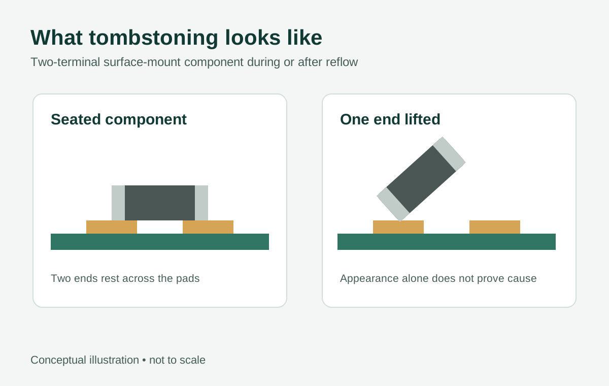
SMT tombstoning occurs when one end of a two-terminal component lifts from its pad during reflow, leaving the part tilted or standing upright. A common mechanism is unequal solder wetting: forces at one termination develop differently from those at the other and pull the component up. Paste deposits, placement, pad geometry, heat flow and surface condition can all contribute, but a lifted component does not identify its own cause.
The most useful response is to preserve evidence from printing through reflow, compare affected and unaffected locations, and test competing explanations one change at a time. Replacing the component may restore one assembly; it does not establish why the defect occurred or whether the next batch is at risk.

What happens during reflow?
A properly seated chip component rests across two paste deposits before reflow. As the solder melts and wets the component terminations and board pads, surface tension helps form the joints. If wetting forces become sufficiently unbalanced while the component can still move, one end may lift away.
Unequal wetting is a useful starting hypothesis, not a complete diagnosis. For example, one pad may heat differently because its copper connection differs from the other. An uneven paste deposit or placement offset can also change the geometry of the developing joints. These conditions can interact: a print that appears acceptable in isolation may still be sensitive to the layout, component and reflow process together.
Other mechanisms can occur, including movement associated with vapor or component flotation in molten solder. A component can also be displaced before or after reflow. Start by confirming when the movement occurred, rather than assuming every lifted part was pulled upright by the same mechanism.
Gather evidence in process order
Investigating in the order the board was built helps distinguish an upstream condition from a reflow effect. Keep affected boards and representative unaffected boards identified until the investigation team agrees what can be inspected or reworked.
1. Confirm the defect and its scope
Record the reference designator, component part number, board revision, panel position and orientation for each affected location. Photograph the component and both pads before disturbing them. Note whether the part is fully upright, partly lifted, shifted or missing, and whether solder is visible on each pad and termination.
Compare similar locations on the same board and on other boards from the lot. A pattern confined to one reference designator points the investigation toward local conditions; defects across unrelated locations may warrant a broader process review. Neither pattern proves a cause on its own.
A lifted end may create an electrical open, but a visual finding and an electrical result answer different questions. Classify and disposition the assembly against the applicable, agreed product and inspection requirements rather than assuming an acceptance rule from appearance alone. For related terminology, see SMT defect classification and solder joint defects.
2. Review the paste deposits before placement
Use available print inspection records or retained pre-placement images to compare the two deposits at the affected location. Look for differences in coverage, position, shape and, where measured, deposit volume or height. Compare the same pads on unaffected boards, and look for changes across panel positions or over time.
Check whether a deposit is offset relative to its pad, not merely whether paste is present. Investigate stencil alignment, aperture condition and cleaning history if the evidence suggests a print problem. Also check the paste identification, handling and use records against the paste supplier’s instructions and the approved process.
A passing print inspection is useful evidence, but it does not eliminate printing or its interaction with the rest of the process. The RIT and SMTA, Case Study: Analyzing 0402 Capacitor Defects and Stencil Printing reported that conventional print criteria passed while defects still occurred, and that orientation mattered in the studied setup. Those observations do not establish a universal print criterion or preferred orientation.
3. Examine placement before reflow
Review placement inspection images or machine records where available. Compare the component center, rotation and overlap with both pads. An offset may leave one termination engaging the paste differently from the other even when the deposits themselves appear similar.
Confirm that the component and footprint match the released design. Check the relevant feeder, nozzle and setup records if an offset repeats. Avoid treating the reflowed position as proof of the original placement position: the component may have moved during melting.
4. Compare the two sides of the footprint
Inspect the released footprint together with the copper connected to each pad. Differences in pad shape, nearby copper, plane connections, traces or vias can change solder distribution or local heat flow. Check the actual board against the design and fabrication records before attributing the issue to the layout.
Do not assume that making pads visually identical will solve the problem. Copper beneath or around the pads, solder-mask definition and the component termination can still make the two sides behave differently. Any footprint or copper revision needs electrical, thermal and assembly review.
5. Measure the thermal process at the relevant location
Review the actual reflow setup and a measured board profile, not just the oven recipe. Where practical, use appropriately attached temperature sensors near the affected location and compare the two sides while recognizing that sensor placement and attachment can affect the reading. Measurements near a pad are evidence of local heating, not a direct measurement of the instant a particular solder joint wets.
Consider board loading, orientation, conveyor conditions and nearby thermal mass. Evaluate the measured ramp, peak, time above the solder’s liquidus and cooling behavior against the applicable paste, component and board requirements. There is no single profile that is correct for every assembly.
6. Check materials and alternative causes
Review board finish and storage history, component condition, paste handling, exposure and any signs of contamination or damage. Compare affected and unaffected material lots where traceability allows. Poor wetting may be relevant, but appearance alone does not establish which surface or material caused it.
Also examine handling and process events that could shift a component before or after reflow. If the available evidence is incomplete, record that limitation and design a test that separates the leading explanations.
Diagnosis matrix: evidence is not a verdict
| Observation | Competing explanations | Useful next check |
|---|---|---|
| Paste appears larger or offset on one pad | Print transfer or alignment issue; pad geometry may also make normal deposits appear different | Compare pre-placement inspection data at the same location across boards. Check stencil alignment and aperture condition before changing the design. |
| Component is offset before reflow | Placement setup or component presentation; uneven paste may also affect how the part sits | Compare placement images with print images. Check repeated offsets and relevant placement records. |
| Pads or surrounding copper differ | Local heat flow or solder distribution may be asymmetric; the defect may instead follow a print or placement pattern | Compare the released layout, actual board features and unaffected matching locations. Measure local heating where practical. |
| Defects correlate with orientation | The assembly may respond to heating direction or another orientation-dependent condition; orientation may also coincide with a specific footprint or panel location | Compare like-for-like locations and measured profiles. If safe and permitted, run a controlled orientation trial without changing the component or footprint at the same time. |
| One side shows weaker wetting or suspect surface condition | Contamination, finish or component condition may contribute; insufficient local heating or other process interactions may produce a similar appearance | Review traceability and handling records; compare material lots and measured heating. Use agreed inspection or analysis methods before assigning blame. |
| Placement and deposits look consistent, but movement appears during or after reflow | Differential wetting is still possible; vapor, flotation or handling may also be involved | Establish the earliest observed movement and compare reflow and handling records. Capture additional process evidence before choosing a corrective action. |
The matrix is a starting point. Several observations can be true at once, and a single image after reflow may not distinguish between them.
Test a change without losing the cause
A useful trial begins with a written hypothesis and a prediction. For example, if the leading hypothesis is that a repeatable placement offset contributes to lifting, compare boards made with the existing placement setting and boards made with a corrected setting, while keeping the other relevant conditions as consistent as practical.
Define which locations will be inspected, what process evidence will be retained and how results will be compared. Include unaffected locations where possible. A small trial can help direct the investigation, but it may not establish long-term process performance. Record the trial conditions and limitations rather than calling a single clean board a proven fix.
Hypothetical example: An assembly team sees lifted capacitors at one footprint. Pre-placement images show similar deposits on both pads, but placement images show a repeatable offset. The team first checks and corrects the placement setup, then builds a comparison under otherwise controlled conditions. If the offset disappears but lifting continues, the placement hypothesis is weakened; the team should return to the layout, thermal and material evidence rather than continuing to adjust placement blindly.
“One variable at a time” is a discipline for interpretable early tests, not a claim that variables act independently. If individually controlled changes do not explain the defect, interactions may need a planned broader experiment. Record any unavoidable changes between runs.
Orientation trials need particular care. Rotate a component only if its electrical function, construction, footprint and product requirements permit it. Rotating a board through the oven can change more than one exposure condition, so document what changed and compare the relevant measurements. Neither rotation is a default remedy.
Turn the finding into a build decision
Different causes lead to different actions:
- Print-related evidence: Review stencil alignment, aperture condition, paste handling and the inspection method. If an aperture change is proposed, assess effects on neighboring joints and obtain the necessary approval.
- Placement-related evidence: Correct the identified setup issue and verify placement before reflow. Check that the corrective action applies to the affected component and locations.
- Layout-related evidence: Review pad and copper balance with the design owner. A board revision may require electrical and fabrication review as well as an assembly trial.
- Thermal-related evidence: Adjust the process only within the applicable material and component requirements, then measure the resulting profile on the relevant assembly.
- Material or surface-related evidence: Segregate suspect material as appropriate, preserve traceability and agree on an investigation with the responsible supplier. Do not assume a finish change alone is the answer.
Rework should follow the agreed product and material requirements. Document what was removed or replaced, inspect the site for damage, and verify the reworked assembly using the applicable criteria. If the cause remains unresolved, keep the containment decision separate from any claim that the process has been corrected.
Paste choice is also part of the process, rather than a substitute for diagnosis. The solder paste selection discussion can help frame the material questions; the selected paste still has to be evaluated with the actual board, component, print and reflow conditions.
What to send with an assembly inquiry
For an actionable discussion with APTPCB, provide the board revision and assembly files, the affected component part numbers and reference designators, and photographs or inspection records identified by process stage. Include the applicable inspection and acceptance requirements, material and lot traceability where available, and the measured reflow information if a build has already been attempted.
State whether the immediate need is to investigate an existing defect, review a proposed design or discuss a new build. Identify any constraints on footprint changes, component rotation, rework and trial quantities. Do not substitute a reflowed-board photo for pre-reflow evidence if the latter is available.
You can start a build inquiry through the quote page or use contact to discuss what information is available.
Public technical references
- RIT and SMTA, Case Study: Analyzing 0402 Capacitor Defects and Stencil Printing — a case-specific investigation of printing, orientation and defects.
- Indium, The Printed Circuit Assembler’s Guide to Solder Defects — supplementary discussion of solder defects and unequal wetting.
- Metallic Resources, Tombstoning Explained — discussion of tombstoning mechanisms, including alternatives to unequal wetting.