
A cold solder joint is a connection where the solder did not fully melt, flow, and wet both the pad and the component lead. It typically looks dull, grainy, or lumpy, with a poor fillet or a visible gap at the edge, and it can pass a quick electrical check while failing later under heat or vibration. Cold joints sit alongside a handful of other solder joint defects that cause most assembly failures: solder bridges, solder balls, cracked joints, and dry or non-wetted joints.
This guide works from the symptom back to the cause. For each defect it shows what it looks like, what usually causes it in reflow, wave, or hand soldering, which inspection method finds it, and how acceptance is normally decided under IPC-A-610. It covers solder joints only. For bare-board defects and a wider failure overview, see the common PCB defects guide.
Key takeaways
- Most solder joint defects trace back to paste volume, wetting, heat, or mechanical stress. Fix the cause, not only the joint.
- Cold and disturbed joints come from too little heat or movement during solidification. Dry or non-wetted joints come from contaminated or oxidized surfaces.
- Bridges and solder balls are usually paste-printing or profile problems in reflow, and flux, preheat, or design problems in wave soldering.
- Cracked joints often appear after assembly, from thermal cycling, board flexing, or vibration. They can be invisible until the product fails.
- AOI catches most visible defects, X-ray is needed for hidden joints under BGAs and QFNs, and electrical test finds opens and shorts but not marginal joints.
- Acceptance depends on the IPC-A-610 class and revision on your drawing. Rework only defects, not acceptable conditions.
Solder joint defect diagnosis table
Use this table first. Find the symptom you see, then follow the row to the likely cause and the inspection method that will confirm it.
| Defect | What it looks like | Most likely root cause | Inspection that catches it | Typical IPC-A-610 disposition (Class 2 and 3) |
|---|---|---|---|---|
| Cold solder joint | Dull, grainy, or lumpy surface; poor fillet; solder sits on the joint instead of flowing | Not enough heat (low peak, short time above liquidus, large thermal mass, weak iron); contaminated surface | Visual, AOI; may pass electrical test while intermittent | Defect when wetting or fillet requirements are not met; rework |
| Disturbed joint | Wrinkled, cracked, or stress-lined surface | Joint moved while solder was solidifying (conveyor vibration, handling, hand-soldering movement) | Visual, AOI | Defect; reflow or rework |
| Solder bridge | Solder connecting two conductors that should be separate | Excess paste, misprint, stencil smear, tight pitch, low preheat or poor flux in wave | SPI (before reflow), AOI, X-ray under BGAs, electrical test | Defect in all classes; remove |
| Solder balls / beading | Small spheres near the joint or beside chip parts | Paste outgassing, moisture, paste on mask, excessive aperture, fast ramp | AOI, visual; X-ray under packages | Acceptable only when entrapped or encapsulated and not violating minimum electrical clearance; otherwise defect |
| Insufficient solder | Fillet too small; pad or lead not fully covered | Low paste volume, clogged aperture, solder wicking into vias | SPI, AOI | Defect when below the class minimum fillet; add solder |
| Non-wetting | Solder beads up and does not bond to the pad or lead; base metal exposed | Oxidized or contaminated pad or lead, aged finish, wrong flux | Visual, AOI, solderability test of incoming parts | Defect; correct surface, then resolder |
| Dewetting | Solder spread then pulled back, leaving thin film and mounds | Contaminated surface or poor finish under the solder | Visual, magnification | Acceptance depends on extent and location; often defect |
| Cracked or fractured joint | Hairline crack around the lead or through the fillet | Thermal cycling fatigue, board flexure, vibration, brittle intermetallics | Magnification, cross-section, X-ray (sometimes), electrical test under stress | Defect; rework and investigate cause |
| Head-in-pillow (BGA) | Ball rests on paste but did not merge | Warpage, oxidized balls, insufficient paste, profile | X-ray (angled or 3D), cross-section | Defect |
| Voids | Gas pockets inside the joint | Paste chemistry, profile, via-in-pad, large thermal pads | X-ray | Judged against the class and any customer limits |
| Tombstoning | Chip part standing on one end | Uneven heating or paste on the two pads | AOI | Defect |
Treat the disposition column as a starting point, not a substitute for the standard. IPC-A-610 criteria change with the revision, the component type, the termination style, and the product class. Your drawing or contract should state which revision and class apply.
What is a cold solder joint and how do you spot one?
A cold solder joint forms when the solder never reaches a full liquid state long enough to wet both metals, or when it is disturbed as it cools. In reflow this usually means the board or a heavy component did not get enough time above the alloy's melting temperature. In hand soldering it usually means the iron tip was too small or cold for the joint, or solder was melted on the tip and dabbed onto the joint instead of heating the pad and lead together.
Signs of a cold joint:
- A dull, frosty, or grainy surface. Lead-free joints are naturally less shiny than tin-lead joints, so judge texture and shape, not only gloss.
- A convex blob instead of a smooth concave fillet.
- A visible line or gap where the solder meets the lead or pad.
- Intermittent faults that change with temperature or when the board is pressed.
Cold joints are often described as "dry joints" in the UK and in repair work. In assembly inspection, a dry joint is closer to a non-wetted joint: the solder is present but never bonded.
How to prevent them: profile the oven on a populated board with thermocouples on the heaviest parts, keep the time above liquidus inside the paste maker's window, and use iron tips and temperatures suited to the thermal mass in hand soldering. The reflow profile basics and the hand soldering guide cover both.
Solder bridge: causes in reflow vs wave
A solder bridge is a short circuit made of solder. It is always a defect. The causes differ by process.
In reflow soldering, bridges usually start at the printer:
- Too much paste from oversize apertures or a thick stencil
- Paste smeared under the stencil, or a misaligned print
- Slumping from a slow or uneven preheat
- Fine-pitch pads with too little solder mask between them
SPI catches most of these before parts are placed. Stencil aperture reduction and mask webs between fine-pitch pads prevent them. See fine-pitch stencil design rules.
In wave and selective soldering, bridges come from:
- Low preheat or too little flux activity
- Board orientation that drags solder between leads
- Leads too long or too closely spaced
- Missing solder thieves on the trailing edge of a connector row
Solder balls and beading
Solder balls are small spheres of solder that break away from the main joint. Beading is a larger ball that sits beside a chip component, usually under or near its body.
Common causes:
- Moisture in paste or boards that turns to steam during reflow
- Fast ramp rates that make flux outgas violently
- Paste printed onto solder mask or left behind by a dirty stencil underside
- Oversized apertures on chip components, which push paste under the part body
Solder balls are a concern because loose balls can move and short conductors later. Under current IPC-A-610 practice, a solder ball is generally acceptable only if it is entrapped or encapsulated (for example, held by no-clean flux residue or coating) and does not reduce spacing below the minimum electrical clearance. Loose balls are removed. Repeated solder balling is a process indicator worth fixing even when individual balls are acceptable.
Cracked or fractured solder joints
A cracked solder joint has a fracture through or around the fillet. Unlike most other defects, it often develops after the assembly leaves the factory.
Typical causes:
- Thermal cycling. Different expansion rates between the component, the solder, and the board fatigue the joint over many cycles. Large ceramic parts and BGAs on thick boards are common sites.
- Mechanical stress. Board bending during depanelization, ICT fixtures, screw mounting, or connector insertion can crack joints and ceramic capacitors.
- Vibration. Heavy parts without mechanical support fatigue their joints.
- Brittle intermetallics. Excessive time at temperature or certain finish and alloy combinations can weaken the interface.
Cracks are hard to see with AOI. Magnification, angled X-ray, and cross-sections find them, and thermal cycling or vibration testing reveals them in qualification. Prevention is mostly design: support heavy parts, keep stress-sensitive parts away from break-off tabs and mounting holes, and control board flexure in fixtures. The thermal cycling test guide explains how to screen for this.
Dry, insufficient and non-wetted joints
These three are related but not the same:
- Insufficient solder means there is not enough solder to form the required fillet. It usually traces to paste volume or to solder wicking into an open via in the pad.
- Non-wetting means solder never bonded to the surface. Base metal is visible and the solder beads up. The cause is the surface: oxidation, contamination, or an aged or poorly plated finish.
- Dewetting means solder bonded briefly, then pulled back, leaving a thin film with mounds. It also points to a surface problem.
When non-wetting appears on many joints of the same part or board lot, check the parts' storage and solderability, and the board finish, before changing the process. The incoming quality control step is where solderability problems with parts and boards should be caught.
Which inspection catches which defect?
No single method finds every solder joint defect. A practical strategy layers them:
| Method | Finds well | Misses or struggles with |
|---|---|---|
| SPI (solder paste inspection) | Insufficient, excess, or offset paste before reflow, which is the root of many bridges and opens | Anything that happens in placement or reflow |
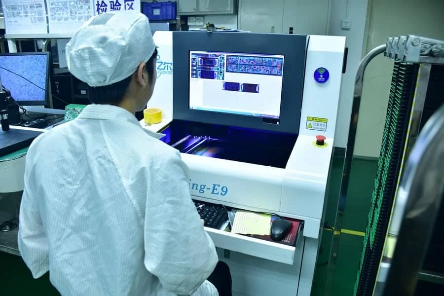
| AOI (automated optical inspection) | Bridges, missing or shifted parts, tombstones, visible fillet problems, polarity | Joints hidden under BGAs, QFNs, and shields; fine cracks |
| X-ray (AXI) | Voids, bridges and opens under BGAs and bottom-terminated parts, head-in-pillow with angled views | Some cracks; wetting quality on visible joints |
| Electrical test (flying probe, ICT) | Opens and shorts, wrong values | Marginal or intermittent joints that still conduct |
| Functional test | Faults that affect operation | Latent defects that fail later |
| Cross-section | Wetting, intermetallics, cracks, voids at any location | It is destructive; used for qualification and failure analysis |
For how these fit into one plan, see the PCBA testing strategy guide. The X-ray criteria for BGA voiding and head-in-pillow cover hidden-joint acceptance in more detail.
Rework or scrap: IPC-A-610 Class 2 vs Class 3
IPC-A-610 sorts each condition into target, acceptable, process indicator, or defect, and the limits get tighter from Class 1 to Class 3. A few practical rules:
- Rework only defects. Reworking an acceptable joint adds heat and can damage pads, parts, and the board.
- Track process indicators. They are not defects, but a rising trend means the process is drifting.
- Class 3 tightens fillet and wetting limits and usually increases inspection coverage, such as X-ray on all BGAs.
- Limit rework cycles. Each heat cycle stresses pads and components. Set a maximum number of rework attempts per location.
- Bridges and non-wetting are defects in every class.
The IPC-A-610 acceptance criteria overview explains classes and conditions, and the IPC Class 2 vs Class 3 assembly guide shows where the two differ in practice.
Process controls to request from your assembler
When you place an order, ask how the assembler controls the causes behind these defects:
- Stencil design rules for fine-pitch and chip parts, and stencil cleaning frequency
- 100% SPI with defined volume, area, and height limits
- Reflow profiles measured on your populated board, with records kept per product
- AOI on every board, and X-ray coverage for BGA, QFN, and other hidden joints
- Moisture-sensitive device handling and baking per J-STD-033
- Incoming solderability checks for suspect parts or aged boards
- A rework procedure with a limit on rework cycles and records by serial or lot
- Defect data (Pareto by defect type) shared with you during NPI and ramp
- The IPC-A-610 class and revision used for acceptance
How APTPCB controls solder joint quality
APTPCB's SMT assembly with AOI and X-ray inspection uses 100% 3D SPI and AOI on its SMT lines, 10-zone nitrogen reflow, and risk-based 3D X-ray for hidden joints, with flying probe, ICT, and functional test available when the build calls for them. Acceptance follows IPC-A-610 and J-STD-001 at the class on your drawing. During NPI, the engineering team reviews footprints, stencil apertures, and the reflow profile for your board, and the inspection results feed back into those settings before volume production. Dedicated X-ray inspection and AOI inspection services cover hidden-joint and visual checks in more depth.
Relevant standards and references may include:
- IPC-A-610: acceptability of electronic assemblies
- J-STD-001: requirements for soldered electrical and electronic assemblies
- IPC-7711/7721: rework, modification and repair of electronic assemblies
- J-STD-002 and J-STD-003: solderability tests for component leads and printed boards
- J-STD-033: handling of moisture-sensitive devices
Frequently asked questions
What causes a cold solder joint?
A cold solder joint is caused by not enough heat or by movement while the solder cools. In reflow it usually means too little time above the solder's melting point on that part. In hand soldering it means the pad and lead were not heated together, or the iron could not deliver enough heat to the joint.
How do you fix a cold solder joint?
Clean the joint, add fresh flux, and reheat the pad and lead together until the solder flows and forms a smooth fillet, adding a little solder if needed. For SMT joints in production, rework follows a controlled procedure, and the process cause should be corrected so the defect does not repeat.
What does a bad solder joint look like?
Bad solder joints may look dull and grainy, lumpy or balled up, cracked, too small to cover the pad, or bridged to a neighboring pin. Lead-free joints are less shiny than tin-lead joints by nature, so shape and wetting matter more than gloss.
What is the difference between a cold joint and a dry joint?
The terms overlap. A cold joint did not get enough heat to flow properly. "Dry joint" is often used for the same thing in repair work, but in inspection it is closer to non-wetting, where solder sits on a surface it never bonded to because of oxidation or contamination.
Are solder balls acceptable under IPC-A-610?
Generally only when they are entrapped or encapsulated and do not reduce spacing below the minimum electrical clearance. Loose solder balls that can move are treated as defects. Check the exact criterion in the IPC-A-610 revision and class on your drawing.
Can X-ray inspection find cracked solder joints?
Sometimes. X-ray finds voids, bridges, and opens under BGAs well, and angled or 3D X-ray can show some cracks and head-in-pillow defects. Fine fatigue cracks are often confirmed only by cross-section or by electrical testing during thermal or mechanical stress.
Fix the cause behind the joint
Every solder joint defect points to a cause: paste volume, wetting, heat, movement, or stress. Use the diagnosis table to name the defect, confirm it with the inspection method that can see it, decide acceptance under the class on your drawing, and then change the process step that created it. That last step is what stops the defect from returning on the next lot.